CY62157ESL MoBL®
Capacitance
Tested initially and after any design or process changes that may affect these parameters.
Parameter | Description | Test Conditions | Max | Unit |
CIN | Input Capacitance | TA = 25°C, f = 1 MHz, VCC = VCC(typ) | 10 | pF |
COUT | Output Capacitance |
| 10 | pF |
Thermal Resistance
Tested initially and after any design or process changes that may affect these parameters.
Parameter | Description | Test Conditions | TSOP II | Unit |
ΘJA | Thermal Resistance | Still Air, soldered on a 3 × 4.5 inch, | 77 | °C/W |
| (Junction to Ambient) | printed circuit board |
|
|
ΘJC | Thermal Resistance |
| 13 | °C/W |
| (Junction to Case) |
|
|
|
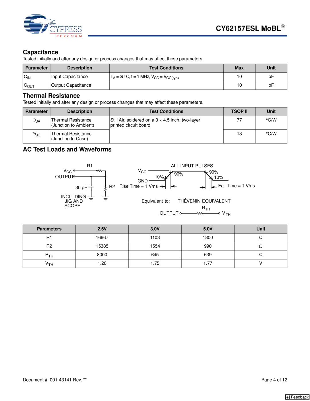
AC Test Loads and Waveforms
R1
VCC ![]()
OUTPUT![]()
30 pF ![]()
INCLUDING
JIG AND
SCOPE
VCC |
|
|
|
|
|
|
|
| ALL INPUT PULSES | |||||||||||
|
|
|
|
|
|
|
|
|
| 90% |
| |||||||||
10% |
|
|
|
|
|
| 90% |
|
|
|
|
|
|
| 10% | |||||
|
|
|
|
|
|
|
|
|
|
|
|
|
|
|
| |||||
GND |
|
|
|
|
|
|
|
|
|
|
|
|
|
|
|
|
| Fall Time = 1 V/ns | ||
|
|
|
|
|
|
|
|
|
|
|
| |||||||||
R2 Rise Time = 1 V/ns |
|
|
|
|
|
|
|
|
|
|
|
|
|
| ||||||
Equivalent to: |
| THÉVENIN EQUIVALENT | ||||||||||||||||||
|
|
|
|
|
|
|
|
|
|
|
| RTH | ||||||||
|
| OUTPUT |
|
|
|
|
|
|
|
|
| V TH | ||||||||
|
|
|
|
|
|
|
|
|
|
| ||||||||||
Parameters | 2.5V | 3.0V | 5.0V | Unit |
R1 | 16667 | 1103 | 1800 | Ω |
|
|
|
|
|
R2 | 15385 | 1554 | 990 | Ω |
|
|
|
|
|
RTH | 8000 | 645 | 639 | Ω |
VTH | 1.20 | 1.75 | 1.77 | V |
Document #: | Page 4 of 12 |
[+] Feedback