CY7C1018DV33
1-Mbit (128K x 8) Static RAM
Features
•Pin- and
•High speed
—tAA = 10 ns
•Low Active Power
—ICC = 60 mA @ 10 ns
•Low CMOS Standby Power
—ISB2 = 3 mA
•2.0V Data retention
•Automatic
•CMOS for optimum speed/power
•Center power/ground pinout
•Easy memory expansion with CE and OE options
•Available in
Functional Description[1]
The CY7C1018DV33 is a
Writing to the device is accomplished by taking Chip Enable (CE) and Write Enable (WE) inputs LOW. Data on the eight I/O pins (I/O0 through I/O7) is then written into the location specified on the address pins (A0 through A16).
Reading from the device is accomplished by taking Chip Enable (CE) and Output Enable (OE) LOW while forcing Write Enable (WE) HIGH. Under these conditions, the contents of the memory location specified by the address pins will appear on the I/O pins.
The eight input/output pins (I/O0 through I/O7) are placed in a
The CY7C1018DV33 is available in
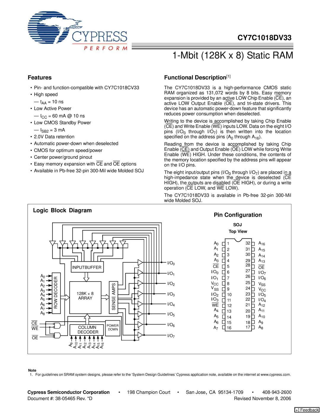
Logic Block Diagram |
|
|
|
|
| Pin Configuration | ||||||||
|
|
|
|
|
|
|
|
|
|
| ||||
|
|
|
|
|
|
|
|
|
|
|
|
| SOJ |
|
|
|
|
|
|
|
|
|
|
|
|
| Top View |
| |
|
|
|
|
|
|
|
|
|
|
| A0 | 1 | 32 | A16 |
|
|
|
|
|
|
|
|
|
|
| A1 | 2 | 31 | A15 |
|
|
|
|
|
|
|
|
|
|
| A2 | 3 | 30 | A |
|
|
|
|
|
|
|
|
|
|
| A3 |
|
| 14 |
|
|
|
|
|
|
|
|
|
| I/O0 | 4 | 29 | A13 | |
| INPUTBUFFER |
| CE | 5 | 28 | OE | ||||||||
|
|
| ||||||||||||
|
|
|
|
|
|
|
|
|
| I/O | I/O0 | 6 | 27 | I/O |
|
|
|
|
|
|
|
|
|
|
|
|
| 7 | |
A0 | ROW DECODER |
|
|
|
|
|
|
|
| 1 | I/O1 | 7 | 26 | I/O6 |
A1 |
|
|
|
|
|
|
| SENSE AMPS | I/O | VCC | 8 | 25 | V | |
A2 |
|
|
|
|
|
|
| 2 | VSS |
| 24 | SS | ||
A |
|
|
|
|
|
|
| I/O3 | 9 | VCC | ||||
A43 | 128K × 8 |
|
| I/O2 | 10 | 23 | I/O5 | |||||||
A5 |
| ARRAY |
|
|
| I/O4 | I/O3 | 11 | 22 | I/O4 | ||||
A6 |
|
|
|
|
|
|
| WE | 12 | 21 | A | |||
A7 |
|
|
|
|
|
|
|
|
| 12 | ||||
|
|
|
|
|
|
|
| A4 | 13 | 20 | A11 | |||
A8 |
|
|
|
|
|
|
|
|
| I/O5 | ||||
|
|
|
|
|
|
|
|
| A5 | 14 | 19 | A10 | ||
CE |
|
| COLUMN |
|
| POWER | I/O6 | A6 | 15 | 18 | A9 | |||
WE |
|
|
|
| A | 16 | 17 | A8 | ||||||
|
| DECODER |
| DOWN |
| 7 |
|
|
| |||||
|
|
|
|
| I/O7 |
|
|
|
| |||||
OE |
|
|
|
|
|
|
|
|
|
|
|
|
| |
| 9 | 10 | 11 | 12 | 13 | 14 | 15 | 16 |
|
|
|
|
|
|
| A A A A A A A A |
|
|
|
|
|
| |||||||
Note |
|
|
|
|
|
|
|
|
|
|
|
|
|
|
1. For guidelines on SRAM system designs, please refer to the ‘System Design Guidelines’ Cypress application note, available on the internet at www.cypress.com.
Cypress Semiconductor Corporation | • 198 Champion Court • San Jose, CA | • | |
Document #: | Revised November 8, 2006 | ||
[+] Feedback