|
|
|
|
|
|
|
|
|
|
|
| CY7C1018DV33 |
| |
|
|
|
|
|
|
|
|
|
|
|
| |||
|
|
|
|
|
|
|
|
|
|
|
|
|
|
|
|
|
|
|
|
|
|
|
|
|
|
|
| ||
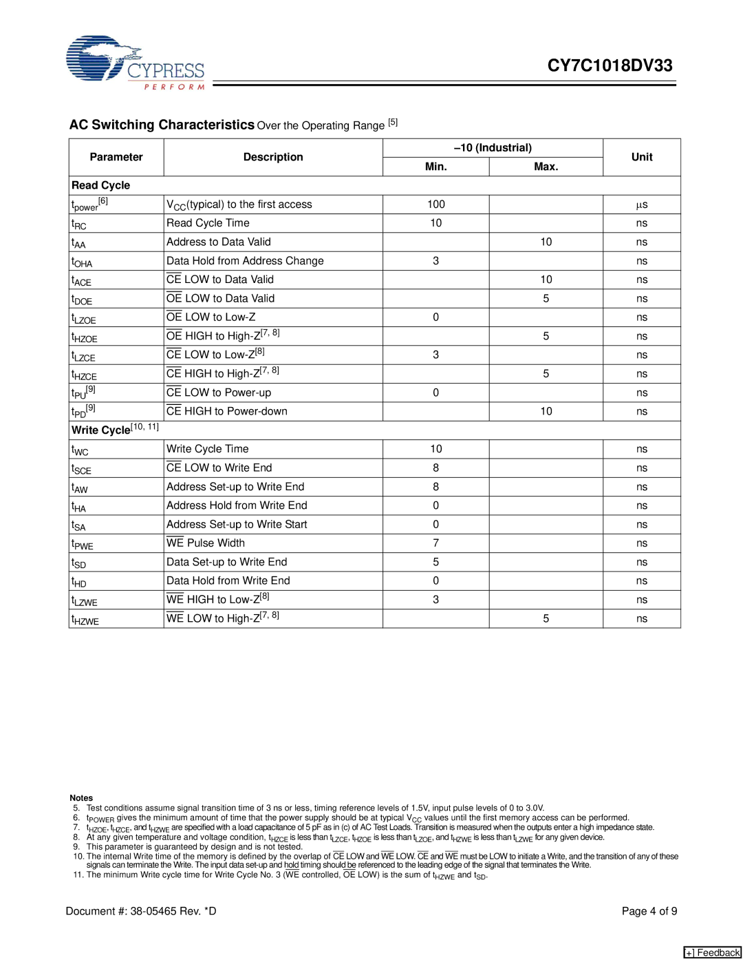
AC Switching Characteristics Over the Operating Range [5] |
|
|
|
|
| |||||||||
| Parameter |
|
|
|
|
|
| Description |
|
|
| Unit |
| |
|
|
|
|
|
|
|
|
|
|
|
| |||
|
|
|
|
|
|
|
| Min. |
| Max. |
| |||
|
|
|
|
|
|
|
|
|
|
|
|
| ||
|
|
|
|
|
|
|
|
|
|
|
|
|
| |
Read Cycle |
|
|
|
|
|
|
|
|
|
|
|
| ||
|
|
|
|
|
|
|
|
| ||||||
tpower[6] |
| VCC(typical) to the first access |
| 100 |
|
| ∝s |
| ||||||
tRC |
| Read Cycle Time |
| 10 |
|
| ns |
| ||||||
tAA |
| Address to Data Valid |
|
|
| 10 | ns |
| ||||||
tOHA |
| Data Hold from Address Change |
| 3 |
|
| ns |
| ||||||
tACE |
|
|
|
| LOW to Data Valid |
|
|
| 10 | ns |
| |||
CE |
|
| ||||||||||||
tDOE |
|
|
|
| LOW to Data Valid |
|
|
| 5 | ns |
| |||
OE |
|
| ||||||||||||
tLZOE |
|
|
|
| LOW to |
| 0 |
|
| ns |
| |||
OE |
|
|
| |||||||||||
tHZOE |
|
|
|
| HIGH to |
|
|
| 5 | ns |
| |||
OE |
|
| ||||||||||||
tLZCE |
|
|
| LOW to |
| 3 |
|
| ns |
| ||||
CE |
|
|
| |||||||||||
tHZCE |
|
|
| HIGH to |
|
|
| 5 | ns |
| ||||
CE |
|
| ||||||||||||
t | [9] |
|
|
| LOW to |
| 0 |
|
| ns |
| |||
CE |
|
|
| |||||||||||
| PU |
|
|
|
|
|
|
|
|
|
|
|
|
|
t | [9] |
|
|
| HIGH to |
|
|
| 10 | ns |
| |||
CE |
|
| ||||||||||||
| PD |
|
|
|
|
|
|
|
|
|
|
|
|
|
Write Cycle[10, 11] |
|
|
|
|
|
|
|
|
|
|
|
|
| |
tWC |
| Write Cycle Time |
| 10 |
|
| ns |
| ||||||
tSCE |
|
|
| LOW to Write End |
| 8 |
|
| ns |
| ||||
CE |
|
|
| |||||||||||
tAW |
| Address |
| 8 |
|
| ns |
| ||||||
tHA |
| Address Hold from Write End |
| 0 |
|
| ns |
| ||||||
tSA |
| Address |
| 0 |
|
| ns |
| ||||||
tPWE |
|
|
|
| Pulse Width |
| 7 |
|
| ns |
| |||
WE |
|
|
| |||||||||||
tSD |
| Data |
| 5 |
|
| ns |
| ||||||
tHD |
| Data Hold from Write End |
| 0 |
|
| ns |
| ||||||
tLZWE |
|
|
|
| HIGH to |
| 3 |
|
| ns |
| |||
WE |
|
|
| |||||||||||
tHZWE |
|
|
|
| LOW to |
|
|
| 5 | ns |
| |||
WE |
|
| ||||||||||||
Notes
5.Test conditions assume signal transition time of 3 ns or less, timing reference levels of 1.5V, input pulse levels of 0 to 3.0V.
6.tPOWER gives the minimum amount of time that the power supply should be at typical VCC values until the first memory access can be performed.
7.tHZOE, tHZCE, and tHZWE are specified with a load capacitance of 5 pF as in (c) of AC Test Loads. Transition is measured when the outputs enter a high impedance state.
8.At any given temperature and voltage condition, tHZCE is less than tLZCE, tHZOE is less than tLZOE, and tHZWE is less than tLZWE for any given device.
9.This parameter is guaranteed by design and is not tested.
10.The internal Write time of the memory is defined by the overlap of CE LOW and WE LOW. CE and WE must be LOW to initiate a Write, and the transition of any of these signals can terminate the Write. The input data
11.The minimum Write cycle time for Write Cycle No. 3 (WE controlled, OE LOW) is the sum of tHZWE and tSD.
Document #: | Page 4 of 9 |
[+] Feedback