CY7C1018DV33
Capacitance[3]
Parameter | Description | Test Conditions | Max. | Unit |
CIN | Input Capacitance | TA = 25°C, f = 1 MHz, VCC = 3.3V | 8 | pF |
COUT | Output Capacitance |
| 8 | pF |
Thermal Resistance[3]
Parameter | Description | Test Conditions |
| Unit | |
Wide SOJ | |||||
|
|
|
| ||
|
|
|
|
| |
ΘJA | Thermal Resistance | Still Air, soldered on a 3 × 4.5 inch, | 57.61 | °C/W | |
| (Junction to Ambient) |
|
| ||
ΘJC | Thermal Resistance |
| 40.53 | °C/W | |
| (Junction to Case) |
|
|
|
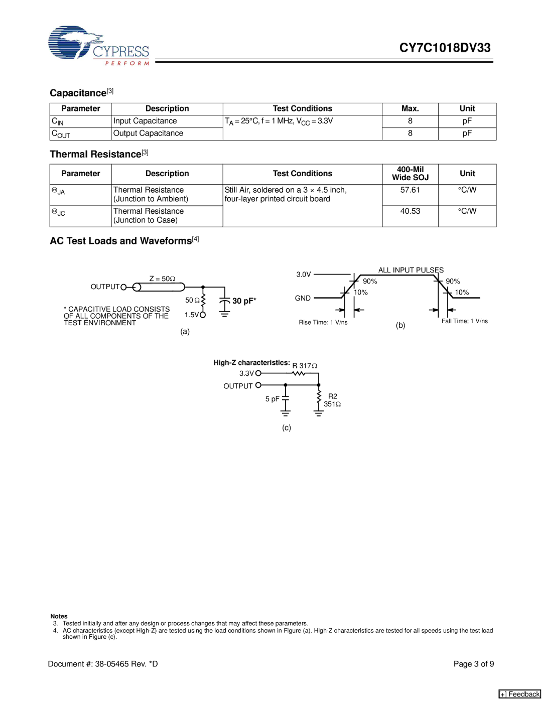
AC Test Loads and Waveforms[4]
Z = 50Ω
OUTPUT |
50 Ω ![]()
* CAPACITIVE LOAD CONSISTS
OF ALL COMPONENTS OF THE 1.5V ![]() TEST ENVIRONMENT
TEST ENVIRONMENT
(a)
3.0V
30 pF* | GND |
Rise Time: 1 V/ns
High-Z characteristics: R 317Ω
3.3V |
OUTPUT |
5 pF |
|
|
|
|
|
|
|
|
|
|
|
| R2 | |
|
|
|
| |||||||||||
|
|
|
|
|
|
|
|
|
|
|
| 351Ω | ||
|
|
|
|
|
|
|
|
|
|
|
|
|
| |
|
|
|
|
|
|
|
|
|
|
|
|
|
|
|
|
|
|
|
|
|
|
|
|
|
|
|
|
|
|
|
|
|
|
|
|
|
|
|
|
|
|
|
|
|
|
|
|
| ALL INPUT PULSES | ||||
|
| 90% |
|
| 90% | |||
|
|
| ||||||
|
|
|
|
| 10% | |||
| 10% | |||||||
|
| |||||||
(b)Fall Time: 1 V/ns
(c)
Notes
3.Tested initially and after any design or process changes that may affect these parameters.
4.AC characteristics (except
Document #: | Page 3 of 9 |
[+] Feedback