|
|
|
|
|
|
|
|
|
|
|
| CY7C1041DV33 | |
|
|
|
|
|
|
|
|
|
|
|
|
| |
|
|
|
|
|
|
|
|
|
|
|
| ||
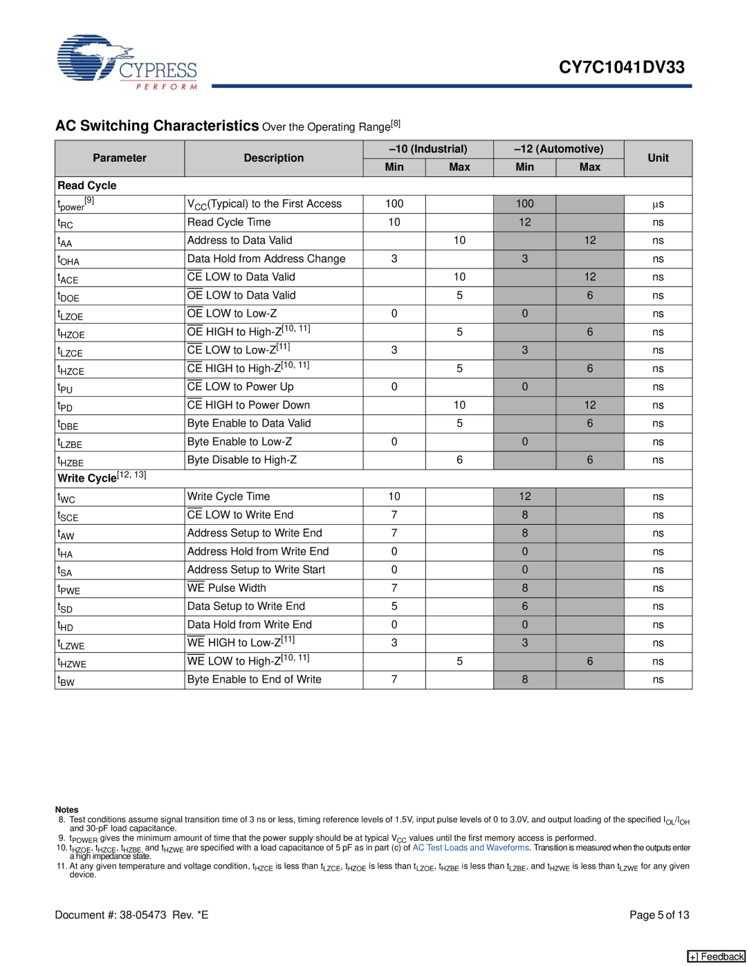
AC Switching Characteristics Over the Operating Range[8] |
|
|
|
| |||||||||
Parameter |
|
|
|
|
|
|
| Description | Unit | ||||
|
|
|
|
|
|
| Min | Max | Min | Max | |||
|
|
|
|
|
|
|
|
|
| ||||
Read Cycle |
|
|
|
|
|
|
|
|
|
|
|
| |
|
|
|
|
|
|
|
|
|
|
|
| ||
tpower[9] |
| VCC(Typical) to the First Access | 100 |
| 100 |
| μs | ||||||
tRC |
| Read Cycle Time | 10 |
| 12 |
| ns | ||||||
tAA |
| Address to Data Valid |
| 10 |
| 12 | ns | ||||||
tOHA |
| Data Hold from Address Change | 3 |
| 3 |
| ns | ||||||
tACE |
|
|
|
|
| LOW to Data Valid |
| 10 |
| 12 | ns | ||
CE |
|
| |||||||||||
tDOE |
|
|
|
|
| LOW to Data Valid |
| 5 |
| 6 | ns | ||
OE |
|
| |||||||||||
tLZOE |
|
|
|
|
| LOW to | 0 |
| 0 |
| ns | ||
OE |
|
| |||||||||||
tHZOE |
|
|
|
|
| HIGH to |
| 5 |
| 6 | ns | ||
OE |
|
| |||||||||||
tLZCE |
|
|
| LOW to | 3 |
| 3 |
| ns | ||||
CE |
|
| |||||||||||
tHZCE |
|
|
| HIGH to |
| 5 |
| 6 | ns | ||||
CE |
|
| |||||||||||
tPU |
|
|
| LOW to Power Up | 0 |
| 0 |
| ns | ||||
CE |
|
| |||||||||||
tPD |
|
|
| HIGH to Power Down |
| 10 |
| 12 | ns | ||||
CE |
|
| |||||||||||
tDBE |
| Byte Enable to Data Valid |
| 5 |
| 6 | ns | ||||||
tLZBE |
| Byte Enable to | 0 |
| 0 |
| ns | ||||||
tHZBE |
| Byte Disable to |
| 6 |
| 6 | ns | ||||||
Write Cycle[12, 13] |
|
|
|
|
|
|
|
|
|
|
|
|
|
tWC |
| Write Cycle Time | 10 |
| 12 |
| ns | ||||||
tSCE |
|
|
| LOW to Write End | 7 |
| 8 |
| ns | ||||
CE |
|
| |||||||||||
tAW |
| Address Setup to Write End | 7 |
| 8 |
| ns | ||||||
tHA |
| Address Hold from Write End | 0 |
| 0 |
| ns | ||||||
tSA |
| Address Setup to Write Start | 0 |
| 0 |
| ns | ||||||
tPWE |
|
|
|
|
| Pulse Width | 7 |
| 8 |
| ns | ||
WE |
|
| |||||||||||
tSD |
| Data Setup to Write End | 5 |
| 6 |
| ns | ||||||
tHD |
| Data Hold from Write End | 0 |
| 0 |
| ns | ||||||
tLZWE |
|
|
|
|
| HIGH to | 3 |
| 3 |
| ns | ||
WE |
|
| |||||||||||
tHZWE |
|
|
|
|
| LOW to |
| 5 |
| 6 | ns | ||
WE |
|
| |||||||||||
tBW |
| Byte Enable to End of Write | 7 |
| 8 |
| ns | ||||||
Notes
8. Test conditions assume signal transition time of 3 ns or less, timing reference levels of 1.5V, input pulse levels of 0 to 3.0V, and output loading of the specified IOL/IOH and
9. tPOWER gives the minimum amount of time that the power supply should be at typical VCC values until the first memory access is performed.
10. tHZOE, tHZCE, tHZBE, and tHZWE are specified with a load capacitance of 5 pF as in part (c) of AC Test Loads and Waveforms. Transition is measured when the outputs enter a high impedance state.
11.At any given temperature and voltage condition, tHZCE is less than tLZCE, tHZOE is less than tLZOE, tHZBE is less than tLZBE, and tHZWE is less than tLZWE for any given device.
Document #: | Page 5 of 13 |
[+] Feedback