CY7C107B

CY7C1007B

Maximum Ratings

(Above which the useful life may be impaired. For user guide- lines, not tested.)

Storage Temperature

− 65°C to +150°C

Ambient Temperature with

− 55°C to +125°C

Power Applied

Current into Outputs (LOW)

20 mA

Static Discharge Voltage

>2001V

(per MIL-STD-883, Method 3015)


Latch-Up Current

>200 mA

Operating Range

Supply Voltage on VCC Relative to GND[1] .....− 0.5V to +7.0V

DC Voltage Applied to Outputs

in High Z State[1]

− 0.5V to VCC + 0.5V

DC Input Voltage[1]

− 0.5V to VCC + 0.5V

Electrical Characteristics Over the Operating Range


Ambient


Range

Temperature[2]

VCC

Commercial

0°C to +70°C

5V ±

10%

Industrial

− 40°C to +85°C

5V ±

10%


7C107B-12

7C107B-15

7C107B-20


7C1007B-12

7C1007B-15

7C1007B-20


Parameter

Description

Test Conditions

Min.

Max.

Min.

Max.

Min.

Max.

Unit


VOH

Output HIGH

VCC = Min., IOH = − 4.0 mA

2.4


2.4


2.4


V


Voltage


VOL

Output LOW

VCC = Min., IOL = 8.0 mA


0.4


0.4


0.4

V


Voltage


VIH

Input HIGH


2.2

VCC+

2.2

VCC+

2.2

VCC+

V


Voltage


0.3


0.3


0.3


VIL

Input LOW


− 0.3

0.8

− 0.3

0.8

− 0.3

0.8

V


Voltage[1]


IIX

Input Load Current

GND < VI < VCC

− 1

+1

− 1

+1

− 1

+1

µ A

IOZ

Output Leakage

GND < VI < VCC,

–5

+5

–5

+5

–5

+5

µ A


Current

Output Disabled


IOS

Output Short

VCC = Max., VOUT = GND


− 300


− 300


− 300

mA


Circuit Current[3]


ICC

VCC Operating

VCC = Max.,


90


80


75

mA


Supply Current

IOUT = 0 mA,


f = fMAX = 1/tRC


ISB1

Automatic


Max. VCC,


> VIH,


20


20


20

mA

CE


CE


Power-Down

VIN >VIH or VIN < VIL,


Current— TTL Inputs

f = f MAX


ISB2

Automatic


Max. VCC,


2


2


2

mA

CE


Power-Down

CE > VCC – 0.3V,


Current—

VIN > VCC – 0.3V or


CMOS Inputs

VIN < 0.3V, f = 0


Notes:

1.VIL (min.) = –2.0V for pulse durations of less than 20 ns.

2.TA is the “Instant On” case temperature.

3.Not more than 1 output should be shorted at one time. Duration of the short circuit should not exceed 30 seconds.

Document #: 38-05030 Rev. **

Page 2 of 9

[+] Feedback

Page 2
Image 2
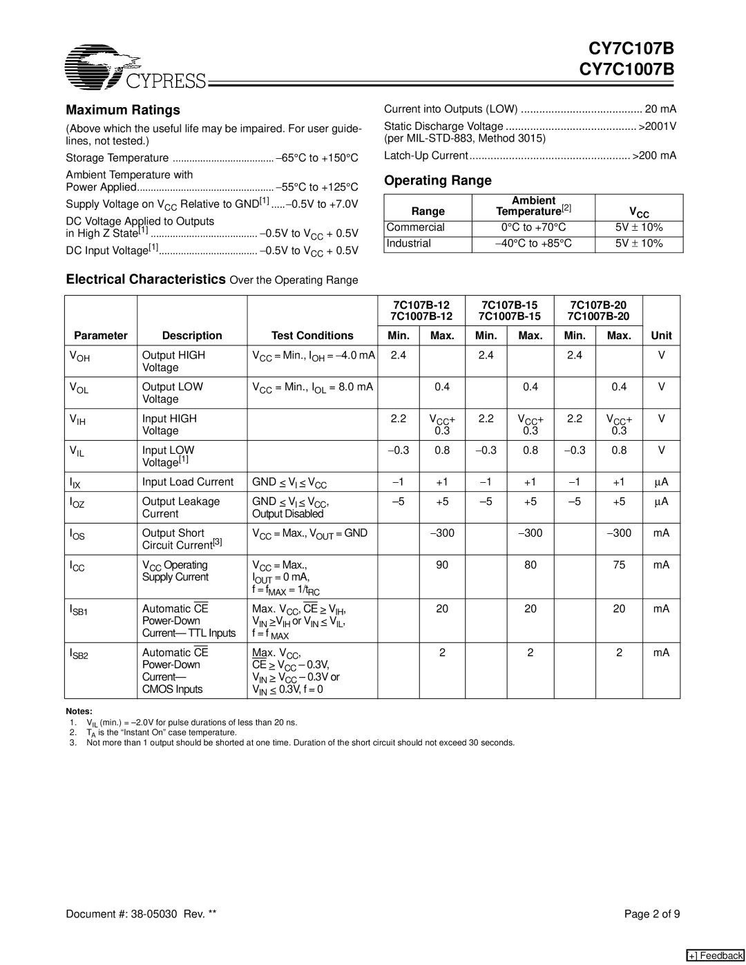
Cypress CY7C107B, CY7C1007B manual Maximum Ratings, Electrical Characteristics Over the Operating Range

CY7C1007B, CY7C107B specifications

Cypress Semiconductor's CY7C107B and CY7C1007B are high-performance static random-access memory (SRAM) devices designed for demanding applications that require fast access times, low power consumption, and high reliability. Both of these memory chips are particularly suitable for use in a variety of electronic systems, including telecommunications, networking, industrial automation, and consumer electronics.

The CY7C107B is a 1 megabit SRAM, while the CY7C1007B is a larger 256 kilobit SRAM. They belong to the Cypress family of asynchronous SRAMs, which are known for their ease of integration into existing systems. One of the main features of these devices is their high-speed operation, with access times that can be as low as 10 nanoseconds. This rapid access allows for quick read and write cycles, making them ideal for applications where speed is critical.

Both memory chips are available in a variety of package options, including 28-pin DIP and 32-pin SOP, allowing for flexible use in different system designs. The CY7C107B and CY7C1007B also employ a dual-port architecture, which enhances their functionality by allowing multiple devices or processors to access the memory simultaneously without conflict. This characteristic is especially beneficial in systems requiring high-throughput data handling, such as video processing or high-speed networking.

Power consumption is another significant aspect of these SRAM devices. They are designed to operate efficiently, with low standby current and minimal active power usage. This makes them suitable for battery-powered and energy-sensitive applications, helping to extend the operating life of such devices.

In terms of reliability, the CY7C107B and CY7C1007B are built using advanced CMOS technology, which not only enhances performance but also increases durability and longevity. These SRAMs are capable of withstanding environmental stresses, thus ensuring consistent performance over time. Furthermore, they incorporate built-in data integrity features to protect against soft errors caused by radiation or other disturbances.

Overall, the Cypress CY7C107B and CY7C1007B SRAMs are robust and efficient solutions for high-speed memory needs. Their combination of fast access times, low power consumption, dual-port capabilities, and reliability makes them excellent choices for a wide range of applications in a rapidly evolving tech landscape. With their proven performance in various sectors, these memory chips continue to be a popular choice among engineers and designers seeking reliable memory solutions.