CY7C1399B

Features

Single 3.3V power supply

Ideal for low-voltage cache memory applications

High speed

10/12/15 ns

Low active power

216 mW (max.)

Low-power alpha immune 6T cell

Plastic SOJ and TSOP packaging

Functional Description

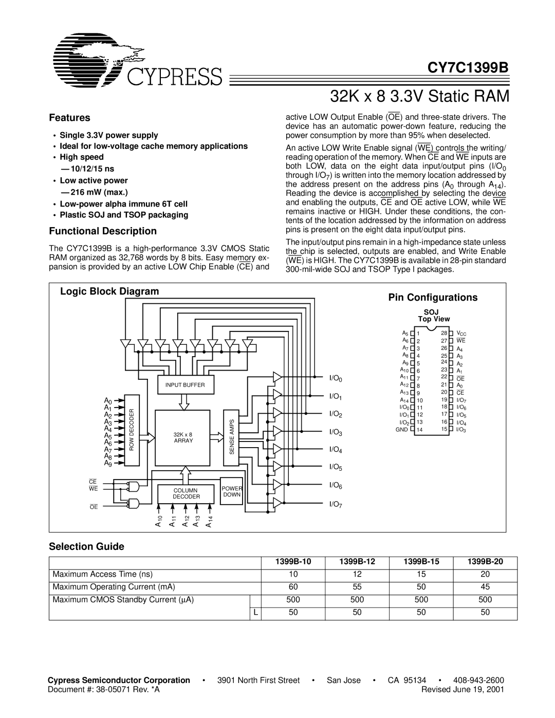
The CY7C1399B is a high-performance 3.3V CMOS Static RAM organized as 32,768 words by 8 bits. Easy memory ex- pansion is provided by an active LOW Chip Enable (CE) and

32K x 8 3.3V Static RAM

active LOW Output Enable (OE) and three-state drivers. The device has an automatic power-down feature, reducing the power consumption by more than 95% when deselected.

An active LOW Write Enable signal (WE) controls the writing/ reading operation of the memory. When CE and WE inputs are both LOW, data on the eight data input/output pins (I/O0 through I/O7) is written into the memory location addressed by the address present on the address pins (A0 through A14). Reading the device is accomplished by selecting the device and enabling the outputs, CE and OE active LOW, while WE remains inactive or HIGH. Under these conditions, the con- tents of the location addressed by the information on address pins is present on the eight data input/output pins.

The input/output pins remain in a high-impedance state unless the chip is selected, outputs are enabled, and Write Enable (WE) is HIGH. The CY7C1399B is available in 28-pin standard 300-mil-wide SOJ and TSOP Type I packages.

Logic Block Diagram


Pin Configurations


SOJ


Top View


A5

1

28

VCC


A6

2

27

WE


A7

3

26

A4


A8

4

25

A


A9


24

3


5

A


A10


23

2


6

A1


I/O0

A11

7

22

OE


INPUT BUFFER


A12

8

21

A


A13

20

0

A


I/O1

9

CE


A14

10

19

I/O7

0


I/O0


I/O6

A


11

18

1

DECODER

32K x 8


AMPS

I/O3

I/O1

12

17

I/O5

A


A2


I/O2

A3


I/O2

13

16

I/O4

A4

ROW


SENSE

I/O4

GND

14

15

I/O3

A7


A65


ARRAY


A8


A9


I/O5


CE


I/O6


WE


COLUMN

POWER


DOWN


DECODER


OE


I/O7


10

11

12

13

14


A

A

A

A

A


Selection Guide


1399B-10

1399B-12

1399B-15

1399B-20


Maximum Access Time (ns)

10

12

15

20


Maximum Operating Current (mA)

60

55

50

45


Maximum CMOS Standby Current (A)


500

500

500

500


L

50

50

50

50


Cypress Semiconductor Corporation • 3901 North First Street

• San Jose • CA 95134 • 408-943-2600

Document #: 38-05071 Rev. *A

Revised June 19, 2001

Page 1
Image 1
Cypress CY7C1399B manual Features, Functional Description, Logic Block Diagram, Selection Guide

CY7C1399B specifications

The Cypress CY7C1399B is a high-performance static random-access memory (SRAM) device that belongs to the family of asynchronous CMOS SRAMs. It is designed to deliver superior speed and efficiency, making it ideal for a multitude of applications in various fields, including telecommunications, automotive, and consumer electronics.

One of the key features of the CY7C1399B is its high-speed operation, capable of achieving access times as low as 12 nanoseconds. This allows for rapid data retrieval, which is crucial in applications requiring fast data processing and real-time performance. Moreover, it operates with a single supply voltage of 2.0V to 3.6V, providing flexibility for power-sensitive designs.

The chip comes with a capacity of 16 megabits, which enables it to store substantial amounts of data. Furthermore, it features a burst mode operation that allows for efficient access to multiple consecutive data locations. This capability makes it particularly useful in applications such as video processing, where quick data retrieval is essential.

Another prominent characteristic of the CY7C1399B is its low power consumption. The device boasts both active and standby power modes, which help minimize energy usage, making it suitable for battery-operated devices. This is increasingly becoming a vital factor for consumer electronics, where energy efficiency is a priority.

In terms of interface, the CY7C1399B uses a conventional parallel interface, compatible with a variety of microcontrollers and processors. The device also supports an asynchronous read and write operation, which simplifies integration into existing systems.

The chip is built using advanced 0.18-micron CMOS technology, which not only enhances its performance but also contributes to its reliability and durability. This technology allows the CY7C1399B to achieve high integration density, resulting in a smaller footprint on printed circuit boards (PCBs).

With a combination of high-speed operational characteristics, low power consumption, and substantial data capacity, the Cypress CY7C1399B stands out as an excellent choice for designers seeking efficient memory solutions that can support the demands of modern electronic systems.