CY7C1561V18, CY7C1576V18
CY7C1563V18, CY7C1565V18
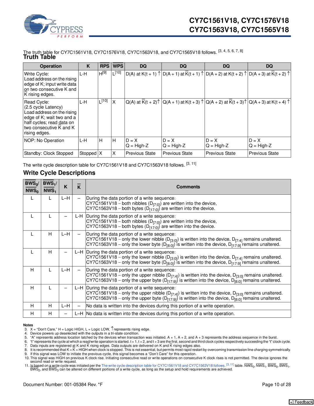
The truth table for CY7C1561V18, CY7C1576V18, CY7C1563V18, and CY7C1565V18 follows. [3, 4, 5, 6, 7, 8]
Truth Table
Operation | K | RPS | WPS | DQ | DQ | DQ | DQ | ||||||||
Write Cycle: | H[9] | L[10] | D(A) at K(t + 1) ↑ | D(A + 1) at |
|
| D(A + 2) at K(t + 2) ↑ |
|
|
| |||||
K(t + 1) ↑ | D(A + 3) at K(t + 2) ↑ | ||||||||||||||
Load address on the rising |
|
|
|
|
|
|
|
|
|
|
|
|
|
|
|
edge of K; input write data |
|
|
|
|
|
|
|
|
|
|
|
|
|
|
|
on two consecutive K and |
|
|
|
|
|
|
|
|
|
|
|
|
|
|
|
K rising edges. |
|
|
|
|
|
|
|
|
|
|
|
|
|
|
|
Read Cycle: | L[10] | X | Q(A) at |
|
| Q(A + 1) at K(t + 3) ↑ |
|
|
| Q(A + 3) at K(t + 4) ↑ | |||||
K(t + 2)↑ | Q(A + 2) at K(t + 3)↑ | ||||||||||||||
(2.5 cycle Latency) |
|
|
|
|
|
|
|
|
|
|
|
|
|
|
|
Load address on the rising |
|
|
|
|
|
|
|
|
|
|
|
|
|
|
|
edge of K; wait two and a |
|
|
|
|
|
|
|
|
|
|
|
|
|
|
|
half cycles; read data on |
|
|
|
|
|
|
|
|
|
|
|
|
|
|
|
two consecutive K and K |
|
|
|
|
|
|
|
|
|
|
|
|
|
|
|
rising edges. |
|
|
|
|
|
|
|
|
|
|
|
|
|
|
|
NOP: No Operation | H | H | D = X | D = X | D = X | D = X | |||||||||
|
|
|
| Q = | Q = | Q = | Q = | ||||||||
Standby: Clock Stopped | Stopped | X | X | Previous State | Previous State | Previous State | Previous State | ||||||||
|
|
|
|
|
|
|
|
|
|
|
|
|
|
|
|
The write cycle description table for CY7C1561V18 and CY7C1563V18 follows. [3, 11]
Write Cycle Descriptions
| BWS0/ | BWS1/ | K |
|
|
| Comments |
|
| |||
|
| K |
|
| ||||||||
|
|
|
|
|
|
|
|
| ||||
| NWS0 |
| NWS1 |
|
| |||||||
|
|
|
|
|
|
|
|
| ||||
| L |
| L |
| – | During the data portion of a write sequence: |
|
| ||||
|
|
|
|
|
|
|
|
|
| CY7C1561V18 − both nibbles (D[7:0]) are written into the device, |
|
|
|
|
|
|
|
|
|
|
|
| CY7C1563V18 − both bytes (D[17:0]) are written into the device. |
|
|
| L |
| L | – | During the data portion of a write sequence: |
|
| |||||
|
|
|
|
|
|
|
|
|
| CY7C1561V18 − both nibbles (D[7:0]) are written into the device, |
|
|
|
|
|
|
|
|
|
|
|
| CY7C1563V18 − both bytes (D[17:0]) are written into the device. |
|
|
| L |
| H |
| – | During the data portion of a write sequence: |
|
| ||||
|
|
|
|
|
|
|
|
|
| CY7C1561V18 − only the lower nibble (D[3:0]) is written into the device, D[7:4] | remains unaltered. | |
|
|
|
|
|
|
|
|
|
| CY7C1563V18 − only the lower byte (D[8:0]) is written into the device, D[17:9] | remains unaltered. | |
| L |
| H | – | During the data portion of a write sequence: |
|
| |||||
|
|
|
|
|
|
|
|
|
| CY7C1561V18 − only the lower nibble (D[3:0]) is written into the device, D[7:4] | remains unaltered. | |
|
|
|
|
|
|
|
|
|
| CY7C1563V18 − only the lower byte (D[8:0]) is written into the device, D[17:9] | remains unaltered. | |
| H |
| L |
| – | During the data portion of a write sequence: |
|
| ||||
|
|
|
|
|
|
|
|
|
| CY7C1561V18 − only the upper nibble (D[7:4]) is written into the device, D[3:0] | remains unaltered. | |
|
|
|
|
|
|
|
|
|
| CY7C1563V18 − only the upper byte (D[17:9]) is written into the device, D[8:0] | remains unaltered. | |
| H |
| L | – | During the data portion of a write sequence: |
|
| |||||
|
|
|
|
|
|
|
|
|
| CY7C1561V18 − only the upper nibble (D[7:4]) is written into the device, D[3:0] | remains unaltered. | |
|
|
|
|
|
|
|
|
|
| CY7C1563V18 − only the upper byte (D[17:9]) is written into the device, D[8:0] | remains unaltered. | |
| H |
| H |
| – | No data is written into the devices during this portion of a write operation. |
|
| ||||
|
|
|
|
|
|
|
|
| ||||
| H |
| H | – | No data is written into the devices during this portion of a write operation. |
|
| |||||
|
|
|
|
|
|
|
|
|
|
|
|
|
Notes
3.X = “Don't Care,” H = Logic HIGH, L = Logic LOW, ↑represents rising edge.
4.Device powers up deselected with the outputs in a
5.“A” represents address location latched by the devices when transaction was initiated. A + 1, A + 2, and A + 3 represents the address sequence in the burst.
6.“t” represents the cycle at which a read/write operation is started. t + 1, t + 2, and t + 3 are the first, second and third clock cycles respectively succeeding the “t” clock cycle.
7.Data inputs are registered at K and K rising edges. Data outputs are delivered on K and K rising edges also.
8.It is recommended that K = K = HIGH when clock is stopped. This is not essential, but permits most rapid restart by overcoming transmission line charging symmetrically.
9.If this signal was LOW to initiate the previous cycle, this signal becomes a “Don’t Care” for this operation.
10.This signal was HIGH on previous K clock rise. Initiating consecutive read or write operations on consecutive K clock rises is not permitted. The device ignores the second read or write request.
11.Is based on a write cycle was initiated per the The write cycle description table for CY7C1561V18 and CY7C1563V18 follows. [3, 11] table. NWS0, NWS1, BWS0, BWS1, BWS2, and BWS3 can be altered on different portions of a write cycle, as long as the setup and hold requirements are achieved.
Document Number:
[+] Feedback