fax id: 1013
CY7C185
Features
•High speed
—15 ns
•Fast t DOE
•Low active power
—715 mW
•Low standby power
—220 mW
•CMOS for optimum speed/power
•Easy memory expansion with CE1, CE2, and OE features
•
•Automatic
Functional Description
The CY7C185 is a
8K x 8 Static RAM
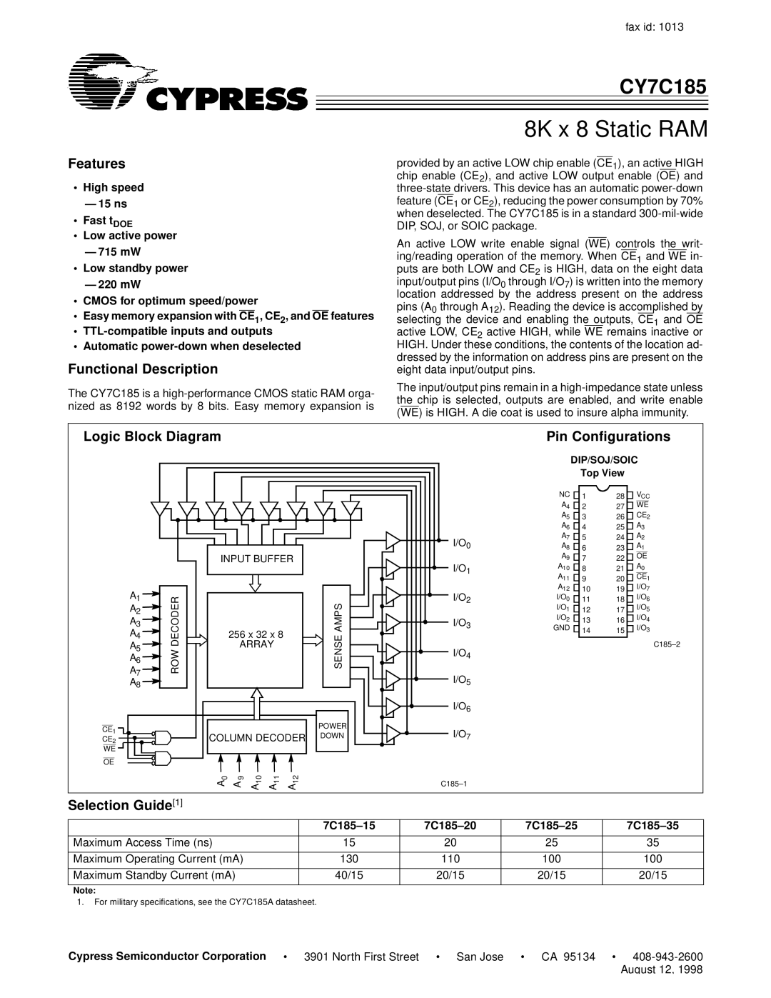
provided by an active LOW chip enable (CE1), an active HIGH chip enable (CE2), and active LOW output enable (OE) and
An active LOW write enable signal (WE) controls the writ- ing/reading operation of the memory. When CE1 and WE in- puts are both LOW and CE2 is HIGH, data on the eight data input/output pins (I/O0 through I/O7) is written into the memory location addressed by the address present on the address pins (A0 through A12). Reading the device is accomplished by
selecting the device and enabling the outputs, CE1 and OE active LOW, CE2 active HIGH, while WE remains inactive or HIGH. Under these conditions, the contents of the location ad- dressed by the information on address pins are present on the eight data input/output pins.
The input/output pins remain in a
Logic Block Diagram | Pin Configurations |
|
|
|
|
|
|
| I/O0 | |
| INPUT BUFFER |
| I/O1 | |||||
|
|
|
|
|
|
| ||
A1 | ROW DECODER |
|
|
|
| SENSE AMPS | I/O2 | |
A2 |
|
|
|
|
| |||
A3 |
|
|
|
| I/O3 | |||
A4 | 256 x 32 x 8 |
|
| |||||
A5 | ARRAY |
| I/O4 | |||||
A6 |
|
|
|
| ||||
A7 |
|
|
|
| I/O5 | |||
A |
|
|
|
|
|
| ||
8 |
|
|
|
|
|
|
| |
|
|
|
|
|
|
| I/O6 | |
CE1 |
|
|
|
|
| POWER | I/O7 | |
COLUMN DECODER | DOWN | |||||||
CE2 | ||||||||
WE |
|
|
|
|
|
|
| |
OE |
|
|
|
|
|
|
| |
| 0 | 9 | 10 | 11 | 12 |
| ||
| A | A | A | A | A |
| ||
|
|
| ||||||
DIP/SOJ/SOIC
Top View
NC | 1 | 28 | VCC |
A4 | 2 | 27 | WE |
A5 | 3 | 26 | CE2 |
A6 | 4 | 25 | A3 |
A7 | 5 | 24 | A2 |
A8 | 6 | 23 | A1 |
A9 | 7 | 22 | OE |
A10 | 8 | 21 | A0 |
A11 | 9 | 20 | CE1 |
A12 | 10 | 19 | I/O7 |
I/O0 | 11 | 18 | I/O6 |
I/O1 | 12 | 17 | I/O5 |
I/O2 | 13 | 16 | I/O4 |
GND | 14 | 15 | I/O3 |
Selection Guide[1]
|
|
|
|
|
|
|
|
|
|
Maximum Access Time (ns) | 15 | 20 | 25 | 35 |
|
|
|
|
|
Maximum Operating Current (mA) | 130 | 110 | 100 | 100 |
|
|
|
|
|
Maximum Standby Current (mA) | 40/15 | 20/15 | 20/15 | 20/15 |
|
|
|
|
|
Note: |
|
|
|
|
1.For military specifications, see the CY7C185A datasheet.
Cypress Semiconductor Corporation • 3901 North First Street • San Jose • CA 95134 •