CY7C185
Switching Waveforms
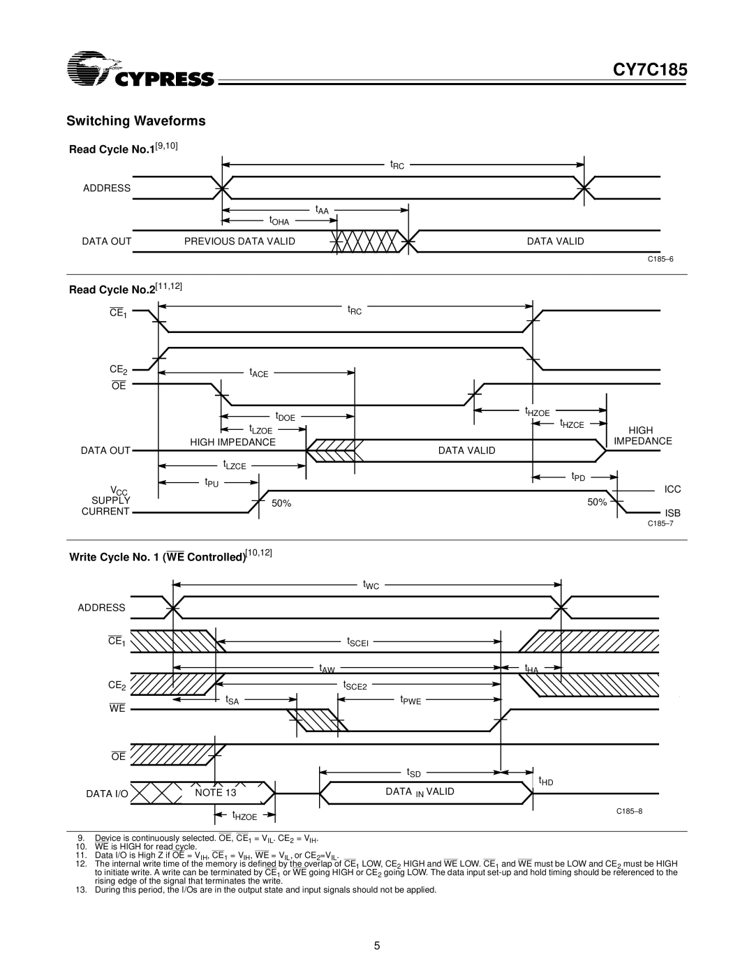
Read Cycle No.1[9,10]
tRC
ADDRESS
tAA
tOHA
DATA OUT | PREVIOUS DATA VALID |
DATA VALID
Read Cycle No.2[11,12] |
|
|
|
CE1 |
| tRC |
|
CE2 | t |
|
|
| ACE |
|
|
OE |
|
|
|
| tDOE | tHZOE |
|
| tHZCE |
| |
| tLZOE | HIGH | |
|
| ||
DATA OUT | HIGH IMPEDANCE | DATA VALID | IMPEDANCE |
|
| ||
| tLZCE | tPD |
|
| tPU |
| |
VCC |
| ICC | |
SUPPLY | 50% |
| 50% |
CURRENT |
|
| ISB |
|
|
|
Write Cycle No. 1 (WE Controlled)[10,12]
tWC
ADDRESS
CE1 ![]()
![]()
![]()
![]() tSCEI
tSCEI
| tAW |
| tHA |
|
|
|
| ||
|
|
|
|
|
CE2 |
|
| tSCE2 |
| ||||||||
|
| |||||||||||
|
|
|
|
|
| tSA |
|
|
|
|
| tPWE |
|
|
|
|
|
|
|
|
|
|
| ||
|
|
|
|
|
| |||||||
WE
OE |
|
|
|
|
| tSD | tHD |
|
| DATA IN VALID | |
DATA I/O | NOTE 13 |
| |
| tHZOE |
| |
|
|
|
9.Device is continuously selected. OE, CE1 = VIL. CE2 = VIH.
10.WE is HIGH for read cycle.
11.Data I/O is High Z if OE = VIH, CE1 = VIH, WE = VIL, or CE2=VIL.
12.The internal write time of the memory is defined by the overlap of CE1 LOW, CE2 HIGH and WE LOW. CE1 and WE must be LOW and CE2 must be HIGH to initiate write. A write can be terminated by CE1 or WE going HIGH or CE2 going LOW. The data input
13.During this period, the I/Os are in the output state and input signals should not be applied.
5