CY7C199
Features
•High speed
—10 ns
•Fast tDOE
•CMOS for optimum speed/power
•Low active power
—467 mW (max, 12 ns “L” version)
•Low standby power
—0.275 mW (max, “L” version)
•2V data retention (“L” version only)
•Easy memory expansion with CE and OE features
•
•Automatic
Functional Description
The CY7C199 is a
32K x 8 Static RAM
provided by an active LOW Chip Enable (CE) and active LOW Output Enable (OE) and
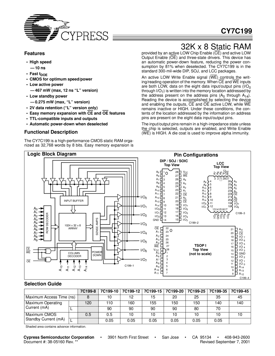
An active LOW Write Enable signal (WE) controls the writ- ing/reading operation of the memory. When CE and WE inputs are both LOW, data on the eight data input/output pins (I/O0 through I/O7) is written into the memory location addressed by the address present on the address pins (A0 through A14). Reading the device is accomplished by selecting the device and enabling the outputs, CE and OE active LOW, while WE remains inactive or HIGH. Under these conditions, the con- tents of the location addressed by the information on address pins are present on the eight data input/output pins.
The input/output pins remain in a
Logic Block Diagram |
|
|
|
|
| Pin Configurations |
|
|
|
|
| |||||||
|
|
|
|
|
|
|
| DIP / SOJ / SOIC |
|
| LCC |
|
|
| ||||
|
|
|
|
|
|
|
| Top View |
|
|
|
|
|
| ||||
|
|
|
|
|
|
|
|
|
|
| Top View |
|
| |||||
|
|
|
|
|
|
|
|
|
|
|
|
|
|
| ||||
|
|
|
|
|
|
| A5 | 1 | 28 | VCC |
|
| 7 6 5 | CC | WE |
|
| |
|
|
|
|
|
|
| A6 | 2 | 27 | WE |
|
| A A A | V |
|
| ||
|
|
|
|
|
|
|
|
| 3 2 1 28 27 |
|
| |||||||
|
|
|
|
|
|
| A7 | 3 | 26 | A4 | A8 | 4 | A4 |
| ||||
|
|
|
|
|
|
| A8 | 4 | 25 | A3 |
|
|
| 26 |
| |||
|
|
|
|
|
|
| A9 | 5 |
|
|
| 25 | A3 |
| ||||
|
|
|
|
|
|
| A9 | 5 | 24 | A2 |
|
|
|
| ||||
|
|
|
|
|
|
| A | 6 |
|
|
| 24 | A |
| ||||
|
|
|
|
|
|
| A10 |
| 23 | A1 | 10 | 7 |
|
|
|
| 2 |
|
|
|
|
|
|
|
| 6 | A11 |
|
|
| 23 | A |
| ||||
|
|
|
|
|
|
| A11 |
| 22 |
| A12 | 8 |
|
|
| 22 | 1 |
|
|
|
|
|
|
| I/O0 | 7 | OE |
|
|
| OE |
| |||||
|
|
|
|
|
| A12 | 8 | 21 | A0 | A13 | 9 |
|
|
| 21 | A0 |
| |
|
| INPUT BUFFER |
|
| A13 | 9 | 20 | CE | A14 | 10 |
|
|
| 20 | CE |
| ||
|
|
|
|
|
| I/O1 | A14 | 10 | 19 | I/O7 | I/O0 | 11 |
|
|
| 19 | I/O7 |
|
A0 |
|
|
|
|
| I/O1 | 12 |
|
|
| 18 | I/O6 |
| |||||
|
|
|
|
|
| I/O0 | 11 | 18 | I/O6 |
| 1314151617 |
|
| |||||
A1 | DECODER |
|
|
|
| I/O2 | I/O1 | 12 | 17 | I/O5 |
|
| 2 | 3 4 5 | ||||
A |
|
|
|
| I/O2 | 13 | 16 | I/O4 |
|
| I/O GND | I/O | I/O | I/O |
|
| ||
2 |
|
|
|
|
|
|
|
|
|
| ||||||||
A |
|
|
| AMPS |
|
|
| 15 | I/O3 |
|
|
|
| |||||
A43 | 1024 x 32 x 8 | I/O3 | GND | 14 |
|
|
| |||||||||||
A5 | ROW | SENSE |
| OE | 22 |
|
|
|
|
|
|
|
|
|
| |||
A6 | ARRAY |
|
|
|
|
|
|
|
|
| 21 | A 0 |
| |||||
|
|
| I/O4 | A 1 | 23 |
|
|
|
|
|
|
|
| |||||
A7 |
|
|
|
|
|
|
|
|
|
| 20 | CE |
| |||||
A |
|
|
|
|
|
| A 2 | 24 |
|
|
|
|
|
|
| 19 | I/O 7 | |
8 |
|
|
|
|
|
| A 3 |
|
|
|
|
|
|
|
| |||
A |
|
|
|
|
|
| 25 |
|
|
|
|
|
|
| 18 | I/O | 6 | |
9 |
|
|
|
|
| I/O5 | A 4 | 26 |
|
|
|
|
|
|
|
| ||
|
|
|
|
|
|
|
| TSOP I |
|
|
|
| 17 | I/O 5 | ||||
|
|
|
|
|
|
| WE | 27 |
|
|
|
|
|
| ||||
CE |
|
|
|
|
|
|
|
|
|
|
|
| 16 | I/O 4 | ||||
|
|
|
|
| I/O | VCC | 28 |
|
| Top View |
|
|
|
| 15 | I/O 3 | ||
WE |
| COLUMN | POWER | 6 | A 5 | 1 |
|
| (not to scale) |
|
|
| 14 | GND | ||||
|
| DOWN |
|
|
|
|
|
| ||||||||||
|
| DECODER |
| A 6 | 2 |
|
|
|
|
|
|
| 13 | I/O 2 | ||||
|
|
| I/O |
|
|
|
|
|
|
| ||||||||
OE |
|
|
|
|
| A 7 | 3 |
|
|
|
|
|
|
| 12 | I/O 1 | ||
|
|
|
|
| 7 | A 8 | 4 |
|
|
|
|
|
|
| ||||
|
|
|
|
|
|
|
|
|
|
|
|
| 11 | I/O 0 | ||||
| 10 | 11 | 12 | 13 | 14 | A 9 | 5 |
|
|
|
|
|
|
| 10 | A 14 | ||
|
|
|
|
|
|
|
|
| ||||||||||
| A | A | A | A | A |
| A 10 | 6 |
|
|
|
|
|
|
| 9 | A 13 | |
|
|
|
|
|
|
| A 11 | 7 |
|
|
|
|
|
|
| 8 | A 12 | |
|
|
|
|
|
|
|
|
|
|
|
|
|
|
|
| |||
|
|
|
|
|
|
|
|
|
|
|
|
|
|
|
|
| ||
Selection Guide
|
|
|
| |||||||||||
| Maximum Access Time (ns) |
| 8 | 10 | 12 |
| 15 |
| 20 | 25 |
| 35 | 45 | |
| Maximum Operating |
|
| 120 | 110 | 160 |
| 155 |
| 150 | 150 |
| 140 | 140 |
| Current (mA) | L |
|
| 90 | 90 |
| 90 |
| 90 | 80 |
| 70 |
|
|
|
|
|
|
|
|
| |||||||
| Maximum CMOS |
|
| 0.5 | 0.5 | 10 |
| 10 |
| 10 | 10 |
| 10 | 10 |
| Standby Current (mA) | L |
|
| 0.05 | 0.05 |
| 0.05 |
| 0.05 | 0.05 |
| 0.05 |
|
|
|
|
|
|
|
|
| |||||||
| Shaded area contains advance information. |
|
|
|
|
|
|
|
|
|
| |||
Cypress Semiconductor Corporation | • 3901 North First Street | • | San Jose • | CA 95134 | • | |||||||||
Document #: |
|
|
|
|
|
|
| Revised September 7, 2001 | ||||||