CY7C199
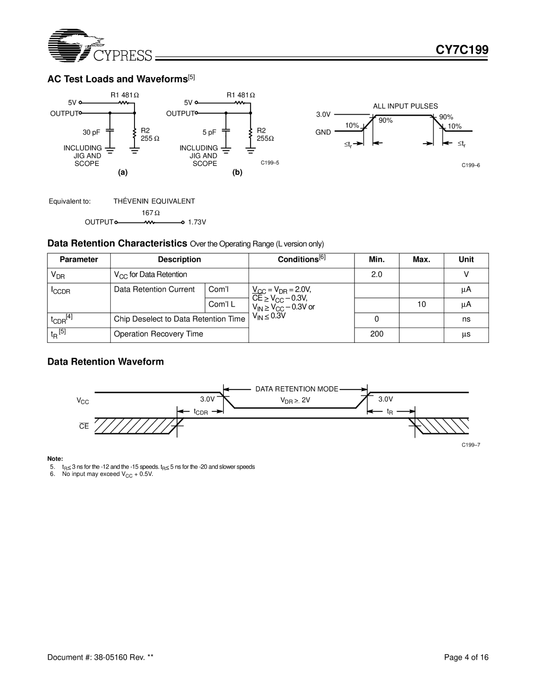
AC Test Loads and Waveforms[5]
R1 481Ω | R1 481Ω |
5V ![]()
OUTPUT![]()
30 pF
INCLUDING
JIG AND
SCOPE
| 5V |
|
|
| |||
|
|
| |||||
R2 | OUTPUT |
|
|
|
|
|
|
5 pF |
|
|
|
|
| ||
|
|
|
|
| |||
|
|
|
|
| |||
255 Ω |
|
|
|
|
|
|
|
INCLUDING
JIG AND
SCOPE
| 3.0V |
|
|
|
| ||
|
|
|
|
| |||
R2 | 10% |
|
|
|
| ||
|
|
|
| ||||
GND |
|
|
|
|
| ||
|
|
|
|
| |||
255Ω |
|
| ≤ tr |
|
|
| |
|
|
|
|
| |||
|
|
|
|
| |||
|
|
|
|
|
|
| |
ALL INPUT PULSES
90% |
| 90% |
| ||
|
|
10%
≤ tr
|
| (a) |
|
|
| (b) |
Equivalent to: | THÉ VENIN EQUIVALENT | |||||
|
|
| 167 Ω | |||
OUTPUT |
|
|
|
| 1.73V | |
|
|
| ||||
Data Retention Characteristics Over the Operating Range (L version only)
Parameter | Description |
|
| Conditions[6] | Min. | Max. | Unit |
VDR | VCC for Data Retention |
|
|
| 2.0 |
| V |
ICCDR | Data Retention Current | Com’l | VCC = VDR = 2.0V, |
|
| ∝ A | |
|
|
| CE > VCC – 0.3V, |
|
|
| |
|
| Com’l L |
| 10 | ∝ A | ||
|
| VIN > VCC – 0.3V or |
| ||||
|
|
|
|
|
| ||
|
|
| V | < 0.3V |
|
|
|
[4] | Chip Deselect to Data Retention Time | 0 |
| ns | |||
tCDR | IN |
| |||||
tR [5] | Operation Recovery Time |
|
|
| 200 |
| ∝ s |
Data Retention Waveform
|
| DATA RETENTION MODE |
|
VCC | 3.0V | VDR > 2V | 3.0V |
| tCDR |
| tR |
CE |
|
|
|
|
|
|
Note:
5.tR< 3 ns for the
6.No input may exceed VCC + 0.5V.
Document #: | Page 4 of 16 |