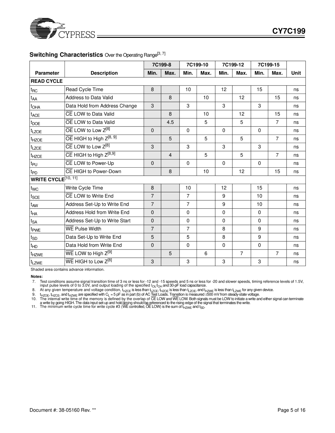
CY7C199
Switching Characteristics Over the Operating Range[3, 7]
|
|
|
|
|
|
| ||||||||
Parameter |
|
|
|
| Description | Min. | Max. | Min. | Max. | Min. | Max. | Min. | Max. | Unit |
READ CYCLE |
|
|
|
|
|
|
|
|
|
|
|
|
| |
|
|
|
|
|
|
|
|
|
|
|
|
|
|
|
tRC |
| Read Cycle Time | 8 |
| 10 |
| 12 |
| 15 |
| ns | |||
tAA |
| Address to Data Valid |
| 8 |
| 10 |
| 12 |
| 15 | ns | |||
tOHA |
| Data Hold from Address Change | 3 |
| 3 |
| 3 |
| 3 |
| ns | |||
tACE |
|
|
|
| LOW to Data Valid |
| 8 |
| 10 |
| 12 |
| 15 | ns |
| CE |
|
|
|
|
|
| |||||||
tDOE |
|
|
|
| LOW to Data Valid |
| 4.5 |
| 5 |
| 5 |
| 7 | ns |
| OE |
|
|
|
|
| ||||||||
tLZOE |
|
|
|
| LOW to Low Z[8] | 0 |
| 0 |
| 0 |
| 0 |
| ns |
| OE |
|
|
|
| |||||||||
tHZOE |
|
|
|
| HIGH to High Z[8, 9] |
| 5 |
| 5 |
| 5 |
| 7 | ns |
| OE |
|
|
|
| |||||||||
t |
|
|
| LOW to Low Z[8] | 3 |
| 3 |
| 3 |
| 3 |
| ns | |
| CE |
|
|
|
| |||||||||
LZCE |
|
|
|
|
|
|
|
|
|
|
|
|
|
|
t |
|
|
| HIGH to High Z[8,9] |
| 4 |
| 5 |
| 5 |
| 7 | ns | |
| CE |
|
|
|
| |||||||||
HZCE |
|
|
|
|
|
|
|
|
|
|
|
|
|
|
tPU |
|
|
|
| LOW to | 0 |
| 0 |
| 0 |
| 0 |
| ns |
| CE |
|
|
|
|
| ||||||||
tPD |
|
|
|
| HIGH to |
| 8 |
| 10 |
| 12 |
| 15 | ns |
| CE |
|
|
|
|
| ||||||||
WRITE CYCLE | [10, 11] |
|
|
|
|
|
|
|
|
| ||||
|
|
|
|
|
|
|
|
|
|
|
|
| ||
tWC |
| Write Cycle Time | 8 |
| 10 |
| 12 |
| 15 |
| ns | |||
tSCE |
|
|
|
| LOW to Write End | 7 |
| 7 |
| 9 |
| 10 |
| ns |
| CE |
|
|
|
|
| ||||||||
tAW |
| Address | 7 |
| 7 |
| 9 |
| 10 |
| ns | |||
tHA |
| Address Hold from Write End | 0 |
| 0 |
| 0 |
| 0 |
| ns | |||
tSA |
| Address | 0 |
| 0 |
| 0 |
| 0 |
| ns | |||
tPWE |
|
|
|
| Pulse Width | 7 |
| 7 |
| 8 |
| 9 |
| ns |
| WE |
|
|
|
| |||||||||
tSD |
| Data | 5 |
| 5 |
| 8 |
| 9 |
| ns | |||
tHD |
| Data Hold from Write End | 0 |
| 0 |
| 0 |
| 0 |
| ns | |||
t |
|
|
|
| LOW to High Z[9] |
| 5 |
| 6 |
| 7 |
| 7 | ns |
| WE |
|
|
|
| |||||||||
HZWE |
|
|
|
|
|
|
|
|
|
|
|
|
|
|
t |
|
|
|
| HIGH to Low Z[8] | 3 |
| 3 |
| 3 |
| 3 |
| ns |
| WE |
|
|
|
| |||||||||
LZWE |
|
|
|
|
|
|
|
|
|
|
|
|
|
|
Shaded area contains advance information.
Notes:
7.Test conditions assume signal transition time of 3 ns or less for
8.At any given temperature and voltage condition, tHZCE is less than tLZCE, tHZOE is less than tLZOE, and tHZWE is less than tLZWE for any given device.
9.tHZOE, tHZCE, and tHZWE are specified with CL = 5 pF as in part (b) of AC Test Loads. Transition is measured ± 500 mV from
10.The internal write time of the memory is defined by the overlap of CE LOW and WE LOW. Both signals must be LOW to initiate a write and either signal can terminate a write by going HIGH. The data input
11.The minimum write cycle time for write cycle #3 (WE controlled, OE LOW) is the sum of tHZWE and tSD.
Document #: | Page 5 of 16 |