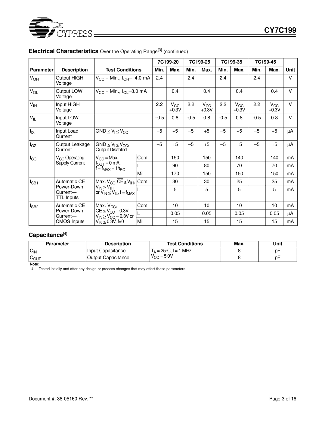
CY7C199
Electrical Characteristics Over the Operating Range[3] (continued)
|
|
|
|
|
|
|
| ||||||||
|
|
|
|
|
|
|
|
|
|
|
|
| |||
Parameter | Description |
| Test Conditions | Min. | Max. | Min. | Max. | Min. | Max. | Min. | Max. | Unit | |||
|
|
|
|
|
|
|
|
|
|
|
| ||||
VOH | Output HIGH | VCC = Min., | 2.4 |
| 2.4 |
| 2.4 |
| 2.4 |
| V | ||||
| Voltage |
|
|
|
|
|
|
|
|
|
|
|
|
|
|
|
|
|
|
|
|
|
|
|
|
|
| ||||
VOL | Output LOW | VCC = Min., IOL=8.0 mA |
| 0.4 |
| 0.4 |
| 0.4 |
| 0.4 | V | ||||
| Voltage |
|
|
|
|
|
|
|
|
|
|
|
|
|
|
|
|
|
|
|
|
|
|
|
|
|
|
|
|
|
|
VIH | Input HIGH |
|
|
|
|
| 2.2 | VCC | 2.2 | VCC | 2.2 | VCC | 2.2 | VCC | V |
| Voltage |
|
|
|
|
|
| +0.3V |
| +0.3V |
| +0.3V |
| +0.3V |
|
|
|
|
|
|
|
|
|
|
|
|
|
|
|
|
|
VIL | Input LOW |
|
|
|
|
| 0.8 | 0.8 | 0.8 | 0.8 | V | ||||
| Voltage |
|
|
|
|
|
|
|
|
|
|
|
|
|
|
|
|
|
|
|
|
|
|
|
|
|
|
| |||
IIX | Input Load | GND < VI < VCC |
| +5 | +5 | +5 | +5 | ∝ A | |||||||
| Current |
|
|
|
|
|
|
|
|
|
|
|
|
|
|
|
|
|
|
|
|
|
|
|
|
|
|
| |||
IOZ | Output Leakage | GND < VI < VCC, |
| +5 | +5 | +5 | +5 | ∝ A | |||||||
| Current | Output Disabled |
|
|
|
|
|
|
|
|
|
| |||
|
|
|
|
|
|
|
|
|
|
|
|
| |||
ICC | VCC Operating | VCC = Max., | Com’l |
| 150 |
| 150 |
| 140 |
| 140 | mA | |||
| Supply Current | IOUT = 0 mA, |
|
|
|
|
|
|
|
|
|
| |||
| L |
| 90 |
| 80 |
| 70 |
| 70 | mA | |||||
|
| f = fMAX = 1/tRC |
|
|
|
|
|
|
|
|
|
| |||
|
| Mil |
| 170 |
| 150 |
| 150 |
| 150 | mA | ||||
|
|
|
|
|
|
|
|
|
| ||||||
|
|
|
|
|
|
|
|
|
|
|
|
| |||
ISB1 | Automatic CE | Max. VCC, |
| >VIH, | Com’l |
| 30 |
| 30 |
| 25 |
| 25 | mA | |
CE |
|
|
|
| |||||||||||
| VIN > VIH |
|
|
|
|
|
|
|
|
|
| ||||
| L |
| 5 |
| 5 |
| 5 |
| 5 | mA | |||||
| Current— | or VIN < VIL, f = fMAX |
|
|
|
|
|
|
|
|
|
| |||
| TTL Inputs |
|
|
|
|
|
|
|
|
|
|
|
|
|
|
|
|
|
|
|
|
|
|
|
|
|
|
| |||
ISB2 | Automatic CE | Max. VCC, | Com’l |
| 10 |
| 10 |
| 10 |
| 10 | mA | |||
| CE > VCC – 0.3V |
|
|
|
|
|
|
|
|
|
| ||||
| L |
| 0.05 |
| 0.05 |
| 0.05 |
| 0.05 | ∝ A | |||||
| Current— | V | > V – 0.3V or |
|
|
|
| ||||||||
|
| IN | CC |
|
|
|
|
|
|
|
|
|
| ||
| CMOS Inputs | VIN < 0.3V, f=0 | Mil |
| 15 |
| 15 |
| 15 |
| 15 | mA | |||
] |
|
|
|
|
|
|
|
|
|
|
|
|
|
|
|
Capacitance[4] |
|
|
|
|
|
|
|
|
|
|
|
|
|
| |
Parameter | Description | Test Conditions | Max. | Unit |
|
|
|
|
|
CIN | Input Capacitance | TA = 25° C, f = 1 MHz, | 8 | pF |
|
| VCC = 5.0V |
|
|
COUT | Output Capacitance | 8 | pF |
Note:
4.Tested initially and after any design or process changes that may affect these parameters.
Document #: | Page 3 of 16 |