CY7C1392BV18, CY7C1992BV18
CY7C1393BV18, CY7C1394BV18
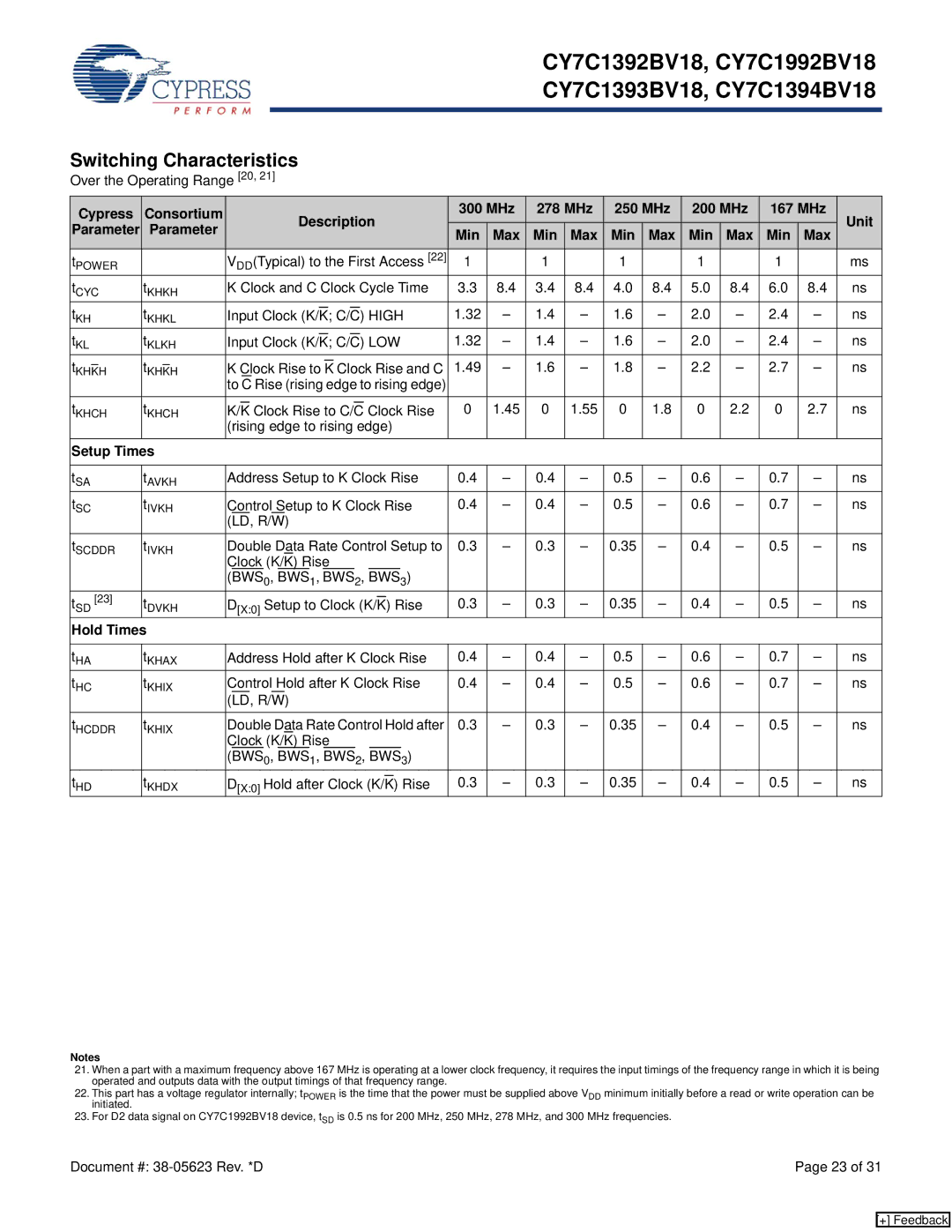
Switching Characteristics
Over the Operating Range [20, 21]
| Cypress | Consortium |
|
|
|
|
| Description | 300 MHz | 278 MHz | 250 MHz | 200 MHz | 167 MHz | Unit | |||||||||||||||||||||||||
Parameter | Parameter |
|
|
|
|
| Min | Max | Min | Max | Min | Max | Min | Max | Min | Max | |||||||||||||||||||||||
|
|
|
|
|
|
|
|
|
|
|
|
|
|
|
|
|
|
|
|
|
|
|
|
|
|
| |||||||||||||
|
|
|
|
|
|
|
|
|
|
|
|
|
|
|
|
|
|
|
|
|
|
|
|
|
|
|
|
|
| ||||||||||
t | POWER |
| V (Typical) to the First Access [22] | 1 |
| 1 |
| 1 |
| 1 |
| 1 |
| ms | |||||||||||||||||||||||||
|
| DD |
|
|
|
|
|
|
|
|
|
|
|
|
|
|
|
|
|
|
|
|
|
|
|
|
|
|
|
|
|
|
|
|
|
| |||
tCYC | tKHKH | K Clock and C Clock Cycle Time | 3.3 | 8.4 | 3.4 | 8.4 | 4.0 | 8.4 | 5.0 | 8.4 | 6.0 | 8.4 | ns | ||||||||||||||||||||||||||
tKH | tKHKL |
|
|
|
|
|
|
|
|
|
|
|
|
|
|
|
|
|
|
|
|
|
|
|
|
|
| 1.32 | – | 1.4 | – | 1.6 | – | 2.0 | – | 2.4 | – | ns | |
Input Clock (K/K; |
| C/C) HIGH | |||||||||||||||||||||||||||||||||||||
tKL | tKLKH |
|
|
|
|
|
|
|
|
|
|
|
|
|
|
|
|
|
|
|
|
|
|
|
|
|
| 1.32 | – | 1.4 | – | 1.6 | – | 2.0 | – | 2.4 | – | ns | |
Input Clock (K/K; |
| C/C) LOW | |||||||||||||||||||||||||||||||||||||
tKHKH | tKHKH | K Clock Rise to |
|
| Clock Rise and C | 1.49 | – | 1.6 | – | 1.8 | – | 2.2 | – | 2.7 | – | ns | |||||||||||||||||||||||
K | |||||||||||||||||||||||||||||||||||||||
|
|
| to C Rise (rising edge to rising edge) |
|
|
|
|
|
|
|
|
|
|
| |||||||||||||||||||||||||
|
|
|
|
|
|
|
|
|
|
|
|
|
|
|
|
|
|
|
|
|
|
|
|
|
|
|
|
|
|
| |||||||||
tKHCH | tKHCH |
|
|
|
|
|
|
|
|
|
|
|
|
|
|
|
|
|
|
|
|
|
|
|
|
|
| 0 | 1.45 | 0 | 1.55 | 0 | 1.8 | 0 | 2.2 | 0 | 2.7 | ns | |
K/K | Clock Rise to C/C Clock Rise | ||||||||||||||||||||||||||||||||||||||
|
|
| (rising edge to rising edge) |
|
|
|
|
|
|
|
|
|
|
| |||||||||||||||||||||||||
Setup Times |
|
|
|
|
|
|
|
|
|
|
|
|
|
|
|
|
|
|
|
|
|
|
|
|
|
|
|
|
|
|
|
|
|
|
|
|
| ||
|
|
|
|
|
|
|
|
|
|
|
|
|
| ||||||||||||||||||||||||||
tSA | tAVKH | Address Setup to K Clock Rise | 0.4 | – | 0.4 | – | 0.5 | – | 0.6 | – | 0.7 | – | ns | ||||||||||||||||||||||||||
tSC | tIVKH | Control Setup to K Clock Rise | 0.4 | – | 0.4 | – | 0.5 | – | 0.6 | – | 0.7 | – | ns | ||||||||||||||||||||||||||
|
|
| (LD, R/W) |
|
|
|
|
|
|
|
|
|
|
| |||||||||||||||||||||||||
tSCDDR | tIVKH | Double Data Rate Control Setup to | 0.3 | – | 0.3 | – | 0.35 | – | 0.4 | – | 0.5 | – | ns | ||||||||||||||||||||||||||
|
|
| Clock (K/K) Rise |
|
|
|
|
|
|
|
|
|
|
| |||||||||||||||||||||||||
|
|
| (BWS0, BWS1, | BWS | 2, | BWS | 3) |
|
|
|
|
|
|
|
|
|
|
| |||||||||||||||||||||
tSD [23] | tDVKH | D |
|
|
|
|
|
|
|
|
|
|
|
|
|
|
|
|
|
|
|
| Rise | 0.3 | – | 0.3 | – | 0.35 | – | 0.4 | – | 0.5 | – | ns | |||||
Setup to Clock (K/K) |
| ||||||||||||||||||||||||||||||||||||||
|
|
| [X:0] |
|
|
|
|
|
|
|
|
|
|
|
|
|
|
|
|
|
|
|
|
|
|
|
|
|
|
|
|
|
|
|
|
|
| ||
Hold Times |
|
|
|
|
|
|
|
|
|
|
|
|
|
|
|
|
|
|
|
|
|
|
|
|
|
|
|
|
|
|
|
|
|
|
|
|
| ||
|
|
|
|
|
|
|
|
|
|
|
|
|
| ||||||||||||||||||||||||||
tHA | tKHAX | Address Hold after K Clock Rise | 0.4 | – | 0.4 | – | 0.5 | – | 0.6 | – | 0.7 | – | ns | ||||||||||||||||||||||||||
tHC | tKHIX | Control | Hold after K Clock Rise | 0.4 | – | 0.4 | – | 0.5 | – | 0.6 | – | 0.7 | – | ns | |||||||||||||||||||||||||
|
|
|
|
|
|
|
|
|
|
|
|
|
|
|
|
|
|
|
|
|
|
| |||||||||||||||||
|
|
| (LD, R/W) |
|
|
|
|
|
|
|
|
|
|
| |||||||||||||||||||||||||
tHCDDR | tKHIX | Double Data Rate Control Hold after | 0.3 | – | 0.3 | – | 0.35 | – | 0.4 | – | 0.5 | – | ns | ||||||||||||||||||||||||||
|
|
| Clock (K/K) Rise |
|
|
|
|
|
|
|
|
|
|
| |||||||||||||||||||||||||
|
|
| (BWS0, BWS1, | BWS | 2, | BWS | 3) |
|
|
|
|
|
|
|
|
|
|
| |||||||||||||||||||||
tHD | tKHDX | D |
|
|
|
|
|
|
|
|
|
|
|
|
|
|
|
|
|
|
|
| Rise | 0.3 | – | 0.3 | – | 0.35 | – | 0.4 | – | 0.5 | – | ns | |||||
Hold after Clock (K/K) | |||||||||||||||||||||||||||||||||||||||
|
|
| [X:0] |
|
|
|
|
|
|
|
|
|
|
|
|
|
|
|
|
|
|
|
|
|
|
|
|
|
|
|
|
|
|
|
|
|
| ||
Notes
21.When a part with a maximum frequency above 167 MHz is operating at a lower clock frequency, it requires the input timings of the frequency range in which it is being operated and outputs data with the output timings of that frequency range.
22.This part has a voltage regulator internally; tPOWER is the time that the power must be supplied above VDD minimum initially before a read or write operation can be initiated.
23.For D2 data signal on CY7C1992BV18 device, tSD is 0.5 ns for 200 MHz, 250 MHz, 278 MHz, and 300 MHz frequencies.
Document #: | Page 23 of 31 |
[+] Feedback