CY7C1392BV18, CY7C1992BV18
CY7C1393BV18, CY7C1394BV18
Switching Waveforms
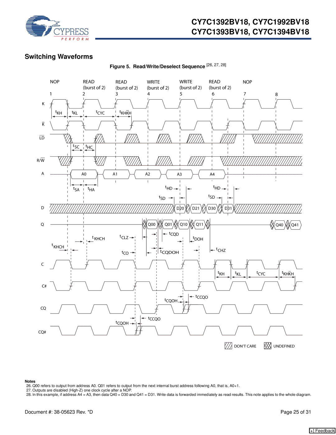
Figure 5. Read/Write/Deselect Sequence [26, 27, 28]
NOP | READ | READ | WRITE | WRITE | READ | NOP |
|
| (burst of 2) | (burst of 2) | (burst of 2) | (burst of 2) | (burst of 2) |
|
|
1 | 2 | 3 | 4 | 5 | 6 | 7 | 8 |
K
K
LD
R/W
A
D
Q
C
|
|
|
|
|
|
|
|
|
|
|
|
|
|
tKH |
| tKL |
| tCYC | tKHKH | ||||||||
|
|
|
|
|
|
|
|
|
|
|
|
|
|
|
|
|
|
|
|
|
|
|
|
|
|
|
|
|
|
|
|
|
|
|
|
|
|
|
|
|
|
tSC
| A0 |
| A1 | A2 |
| A3 |
| A4 |
|
|
t | SA | t | HA |
| tHD |
|
| tHD |
| |
|
|
|
|
|
|
|
|
| ||
|
|
|
|
| tSD |
|
| tSD |
|
|
|
|
|
|
|
| D20 | D21 | D30 | D31 |
|
|
|
|
| Q00 | Q01 | Q10 | Q11 |
| Q40 | Q41 |
|
|
| t KHCH | tCLZ | tCQD | tDOH |
|
|
| |
|
|
|
|
|
|
|
| |||
tKHCH |
|
|
| tCO | tCQDOH |
|
| tCHZ |
| |
|
|
|
|
|
|
| ||||
|
|
|
|
|
|
|
| |||
C#
CQ
CQ#
tCQOH 
tCQOH
 tCCQO
tCCQO
tKH
![]() tCCQO
tCCQO
tKL
tCYC
tKHKH
DON’T CARE
UNDEFINED
Notes
26.Q00 refers to output from address A0. Q01 refers to output from the next internal burst address following A0, that is, A0+1.
27.Outputs are disabled
28.In this example, if address A4 = A3, then data Q40 = D30 and Q41 = D31. Write data is forwarded immediately as read results. This note applies to the whole diagram.
Document #: | Page 25 of 31 |
[+] Feedback
