CY7C291A

CY7C292A/CY7C293A

Switching Characteristics Over the Operating Range[3, 4]


7C291A-25

7C291A-35

7C291A-50


7C292A-25

7C292A-35

7C292A-50


7C293A-25

7C293A-35

7C293A-50


7C291A-20

7C291AL-25

7C291AL-35

7C291AL-50


7C292A-20

7C292AL-25

7C292AL-35

7C292AL-50


7C293A-20

7C293AL-25

7C293AL-35

7C293AL-50


Parameter

Description

Min.

Max.

Min.

Max.

Min.

Max.

Min.

Max.

Unit


Notes:

6.tHZCS2 and tACS2 refer to 7C293A CS1 only.

Erasure Characteristics

Wavelengths of light less than 4000 Angstroms begin to erase these PROMs. For this reason, an opaque label should be placed over the window if the PROM is exposed to sunlight or fluorescent lighting for extended periods of time.

The recommended dose of ultraviolet light for erasure is a wavelength of 2537 Angstroms for a minimum dose (UV inten- sity x exposure time) of 25 Wsec/cm2. For an ultraviolet lamp with a 12 mW/cm2 power rating, the exposure time would be approximately 35 minutes.

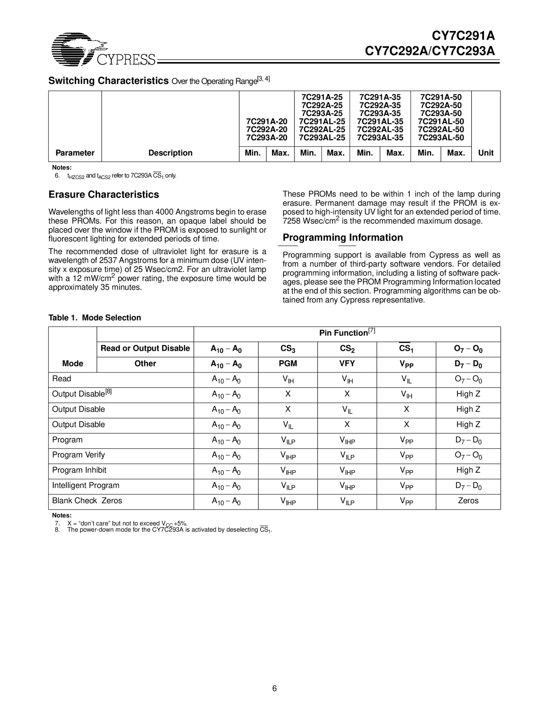
Table 1. Mode Selection

These PROMs need to be within 1 inch of the lamp during erasure. Permanent damage may result if the PROM is ex- posed to high-intensity UV light for an extended period of time. 7258 Wsec/cm2 is the recommended maximum dosage.

Programming Information

Programming support is available from Cypress as well as from a number of third-party software vendors. For detailed programming information, including a listing of software pack- ages, please see the PROM Programming Information located at the end of this section. Programming algorithms can be ob- tained from any Cypress representative.


Pin Function[7]


Read or Output Disable

A10

A0

CS3

CS2


CS1

O7

O0

Mode


Other

A10

A0

PGM

VFY


VPP

D7

D0

Read


A10

A0

VIH

VIH


VIL

O7

O0

Output Disable[8]


A

10

A

X

X


V

IH

High Z


0


Output Disable


A10

A0

X

VIL


X

High Z

Output Disable


A10

A0

VIL

X


X

High Z

Program


A10

A0

VILP

VIHP


VPP

D7

D0

Program Verify


A10

A0

VIHP

VILP


VPP

O7

O0

Program Inhibit


A10

A0

VIHP

VIHP


VPP

High Z

Intelligent Program


A10

A0

VILP

VIHP


VPP

D7

D0

Blank Check Zeros


A10

A0

VIHP

VILP


VPP

Zeros

Notes:

7.X = “don’t care” but not to exceed VCC +5%.

8.The power-down mode for the CY7C293A is activated by deselecting CS1.

6

Page 6
Image 6
Cypress CY7C293A, CY7C291A, CY7C292A manual Erasure Characteristics, Programming Information

CY7C291A, CY7C292A, CY7C293A specifications

The Cypress CY7C293A, CY7C292A, and CY7C291A are high-performance static random-access memory (SRAM) devices designed for various applications requiring fast access and low power consumption. These memory chips are particularly suitable for use in telecommunications, networking, industrial, automotive, and consumer electronics.

One key feature of the CY7C293A model is its 2 megabit capacity, which offers a vast storage solution for applications needing quick read and write capabilities. The CY7C292A and CY7C291A, on the other hand, provide 1 megabit and 256 kilobits, respectively, catering to a range of memory needs. The devices utilize a 16-bit organization, optimally balancing capacity and access speed.

A standout technology is the use of a fast access time, with the CY7C293A achieving speeds of up to 12 nanoseconds. This rapid access capability significantly enhances the performance of systems that depend on swift data retrieval. The SRAM devices are built using Cypress’s unique CMOS technology, which not only supports a dense manufacturing process but also ensures low power consumption. The standby current is minimal, making these chips suitable for battery-powered applications where energy efficiency is critical.

The packaging options available for the CY7C293A, CY7C292A, and CY7C291A include various forms such as 28-pin DIP and 32-pin TSOP, allowing for ease of integration into different circuit layouts. The devices feature an asynchronous operation, providing straightforward interfacing with no need for external clocks, which simplifies system design.

In terms of reliability, these SRAMs are equipped with robust features that ensure data integrity and stability. They offer a wide operating voltage range, typically from 4.5V to 5.5V, accommodating different power supply configurations. Furthermore, the chips are designed to withstand multiple read/write cycles, making them ideal for applications that demand frequent data manipulation.

Overall, the Cypress CY7C293A, CY7C292A, and CY7C291A SRAM devices represent a versatile memory solution that combines speed, efficiency, and reliability, making them a favored choice for engineers and designers working across various technological domains. Their adaptability to different applications ensures that they remain relevant in the rapidly evolving landscape of electronics and memory technology.