|
|
|
|
|
| STK11C68 | |||
Capacitance |
|
|
|
|
|
|
| ||
In the following table, the capacitance parameters are listed.[3] |
|
|
|
|
|
| |||
Parameter | Description | Test Conditions |
| Max |
| Unit | |||
CIN | Input Capacitance | TA = 25°C, f = 1 MHz, |
| 8 |
|
| pF | ||
|
| VCC = 0 to 3.0V |
|
|
|
|
| ||
COUT | Output Capacitance |
| 7 |
|
| pF | |||
Thermal Resistance |
|
|
|
|
|
|
| ||
In the following table, the thermal resistance parameters are listed.[3] |
|
|
|
|
|
| |||
Parameter | Description | Test Conditions |
|
|
| Unit | |||
ΘJA | Thermal Resistance | Test conditions follow standard test methods | TBD | TBD | TBD | °C/W | |||
| (Junction to Ambient) | and procedures for measuring thermal |
|
|
|
|
|
| |
|
| impedance, per EIA / JESD51. |
|
|
|
| |||
ΘJC | Thermal Resistance | TBD | TBD | TBD | °C/W | ||||
| (Junction to Case) |
|
|
|
|
|
|
| |
|
|
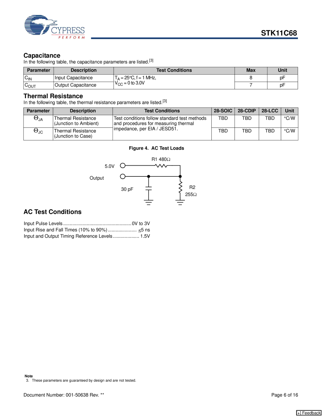
| Figure 4. AC Test Loads |
|
|
|
|
|
|
R1 480Ω
5.0V |
Output |
30 pF |
| R2 |
| ||
|
|
255Ω
AC Test Conditions
Input Pulse Levels | 0V to 3V |
Input Rise and Fall Times (10% to 90%) | <5 ns |
Input and Output Timing Reference Levels | 1.5V |
Note
3. These parameters are guaranteed by design and are not tested.
Document Number: | Page 6 of 16 |
[+] Feedback