nvSRAM Operation
nvSRAM
The STK14D88 nvSRAM is made up of two functional compo- nents paired in the same physical cell. These are the SRAM memory cell and a nonvolatile QuantumTrap™ cell. The SRAM memory cell operates like a standard fast static RAM. Data in the SRAM can be transferred to the nonvolatile cell (the STORE operation), or from the nonvolatile cell to SRAM (the RECALL
STK14D88
VCAP pin is driven to 5V by a charge pump internal to the chip. A pull up should be placed on W to hold it inactive during power up.
To reduce unneeded nonvolatile stores, AutoStore and Hardware Store operations will be ignored unless at least one WRITE operation has taken place since the most recent STORE or RECALL cycle. Software initiated STORE cycles are performed regardless of whether a WRITE operation has taken place. The HSB signal can be monitored by the system to detect an AutoStore cycle is in progress.
operation). This unique architecture allows all cells to be stored and recalled in parallel. During the STORE and RECALL opera- tions SRAM READ and WRITE operations are inhibited. The STK14D88 supports unlimited read and writes like a typical SRAM. In addition, it provides unlimited RECALL operations from the nonvolatile cells and up to 200K STORE operations.
SRAM READ
The STK14D88 performs a READ cycle whenever E and G are low while W and HSB are high. The address specified on pins
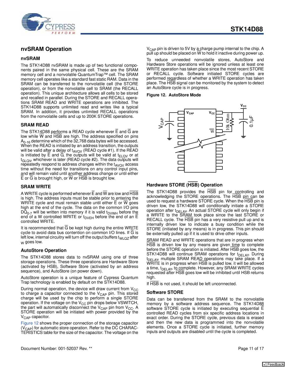
Figure 12. AutoStore Mode
VCAP
CAP
V
VCC
W
| VCC |
10k Ohm | 0.1µF |
SRAM WRITE
A WRITE cycle is performed whenever E and W are low and HSB is high. The address inputs must be stable prior to entering the WRITE cycle and must remain stable until either E or W goes high at the end of the cycle. The data on the common I/O pins
It is recommended that G be kept high during the entire WRITE cycle to avoid data bus contention on common I/O lines. If G is left low, internal circuitry will turn off the output buffers tWLQZ after W goes low.
AutoStore Operation
The STK14D88 stores data to nvSRAM using one of three storage operations. These three operations are Hardware Store (activated by HSB), Software Store (activated by an address sequence), and AutoStore (on power down).
AutoStore operation is a unique feature of Cypress Quantum Trap technology is enabled by default on the STK14D88.
During normal operation, the device will draw current from VCC to charge a capacitor connected to the VCAP pin. This stored charge will be used by the chip to perform a single STORE operation. If the voltage on the VCC pin drops below VSWITCH, the part will automatically disconnect the VCAP pin from VCC. A STORE operation will be initiated with power provided by the VCAP capacitor.
Figure 12 shows the proper connection of the storage capacitor (VCAP) for automatic store operation. Refer to the DC CHARAC- TERISTICS table for the size of the capacitor. The voltage on the
Document Number:
Hardware STORE (HSB) Operation
The STK14D88 provides the HSB pin for controlling and acknowledging the STORE operations. The HSB pin can be used to request a hardware STORE cycle. When the HSB pin is driven low, the STK14D88 will conditionally initiate a STORE operation after tDELAY. An actual STORE cycle will only begin if a WRITE to the SRAM took place since the last STORE or RECALL cycle. The HSB pin has a very resistive pull up and is internally driven low to indicate a busy condition while the STORE (initiated by any means) is in progress. This pin should be externally pulled up if it is used to drive other inputs.
SRAM READ and WRITE operations that are in progress when HSB is driven low by any means are given time to complete before the STORE operation is initiated. After HSB goes low, the STK14D88 will continue SRAM operations for tDELAY. During tDELAY, multiple SRAM READ operations may take place. If a WRITE is in progress when HSB is pulled low, it will be allowed a time, tDELAY, to complete. However, any SRAM WRITE cycles requested after HSB goes low will be inhibited until HSB returns high.
If HSB is not used, it should be left unconnected.
Software STORE
Data can be transferred from the SRAM to the nonvolatile memory by a software address sequence. The STK14D88 software STORE cycle is initiated by executing sequential E controlled READ cycles from six specific address locations in exact order. During the STORE cycle, previous data is erased and then the new data is programmed into the nonvolatile elements. Once a STORE cycle is initiated, further memory inputs and outputs are disabled until the cycle is completed.
Page 11 of 17
[+] Feedback