STK14D88
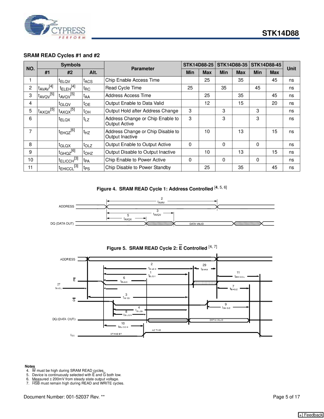
SRAM READ Cycles #1 and #2
NO. |
|
|
|
| Symbols |
| Parameter | Unit | |||||||
| #1 |
| #2 | Alt. | Min | Max | Min | Max | Min | Max | |||||
|
|
|
|
| |||||||||||
1 |
|
|
| tELQV |
| tACS | Chip Enable Access Time |
| 25 |
| 35 |
| 45 | ns | |
2 | tAVAV[4] | tELEH[4] | tRC | Read Cycle Time | 25 |
| 35 |
| 45 |
| ns | ||||
3 | t | AVQV | [5] | t | AVQV | [5] | t | Address Access Time |
| 25 |
| 35 |
| 45 | ns |
|
|
|
|
| AA |
|
|
|
|
|
|
|
| ||
4 |
|
|
| tGLQV | tOE | Output Enable to Data Valid |
| 12 |
| 15 |
| 20 | ns | ||
5 | t |
| [5] | t |
| [5] | t | Output Hold after Address Change | 3 |
| 3 |
| 3 |
| ns |
|
| AXQX |
| AXQX | OH |
|
|
|
|
|
|
|
| ||
6 |
|
|
| tELQX |
| tLZ | Address Change or Chip Enable to | 3 |
| 3 |
| 3 |
| ns | |
|
|
|
|
|
|
|
| Output Active |
|
|
|
|
|
|
|
7 |
|
|
| tEHQZ[6] | tHZ | Address Change or Chip Disable to |
| 10 |
| 13 |
| 15 | ns | ||
|
|
|
|
|
|
|
| Output Inactive |
|
|
|
|
|
|
|
8 |
|
|
| tGLQX | tOLZ | Output Enable to Output Active | 0 |
| 0 |
| 0 |
| ns | ||
9 |
|
|
| tGHQZ[6] | tOHZ | Output Disable to Output Inactive |
| 10 |
| 13 |
| 15 | ns | ||
10 |
|
|
| tELICCH[3] | tPA | Chip Enable to Power Active | 0 |
| 0 |
| 0 |
| ns | ||
11 |
|
|
| tEHICCL[3] | tPS | Chip Disable to Power Standby |
| 25 |
| 35 |
| 45 | ns | ||
Figure 4. SRAM READ Cycle 1: Address Controlled [4, 5, 6]
ADDRESS
DQ (DATA OUT)
2
tAVAV
3
5tAVQV
tAXQX ![]()
![]()
DATA VALID
Figure 5. SRAM READ Cycle 2: E Controlled [4, 7]
2 | 29 |
1 | 11 |
6
7
3
9
4
8
10
Notes
4.W must be high during SRAM READ cycles.
5.Device is continuously selected with E and G both low.
6.Measured ± 200mV from steady state output voltage.
7.HSB must remain high during READ and WRITE cycles.
Document Number: | Page 5 of 17 |
[+] Feedback