J E O L J S M - 6 0 6 0 L V S C A N N I N G E L E C T R O N M I C R O S C O P E | 2 |
Background
The scanning electron microscope (SEM) is one of the most versatile instruments for the examination and analysis of the microstructural characteristics of solids. Although the SEM and optical microscope share the same primary function – making microstructural features and objects visible to the human eye – the scanning electron microscope offers some distinct advantages over the optical microscope. The SEM uses electrons rather than visible light waves (200 – 750 nm wavelength) for imaging, which allows for observation of relatively large sample features at low magnifications or very fine details (high resolution) at high magnifications. The SEM also offers a large depth of field that provides good focus over rough specimen surfaces. The large depth of focus provides a
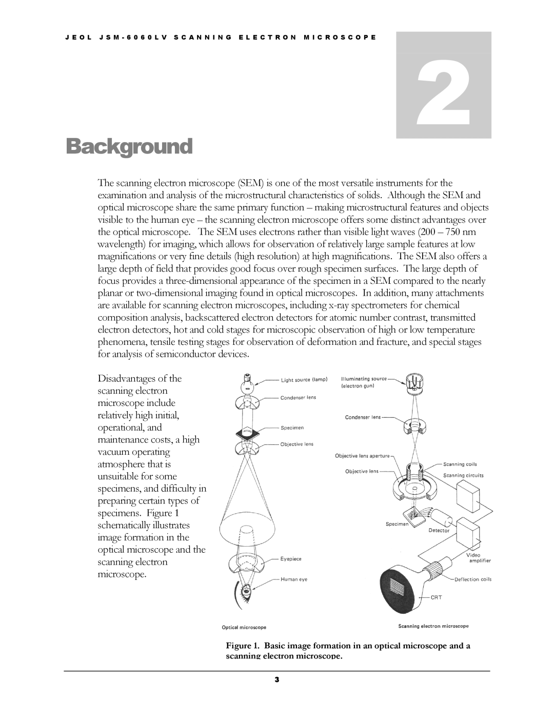
Disadvantages of the scanning electron microscope include relatively high initial, operational, and maintenance costs, a high vacuum operating atmosphere that is unsuitable for some specimens, and difficulty in preparing certain types of specimens. Figure 1 schematically illustrates image formation in the optical microscope and the scanning electron microscope.
Figure 1. Basic image formation in an optical microscope and a scanning electron microscope.
3
