A B O U T T H E D E V E L O P M E N T B O A R D
. . .
U.FL and
assert the W_DISABLE# signal to the module, place a jumper between either pins 18 and 20 or pins 19 and 20.
As an alternative, you can drive this pin with a low voltage TTL or CMOS driver. When asserted, W_DISABLE# lights the DISABLE LED, DS3.
U . F L a n d R P - S M A c o n n e c t o r s
. . . . . . . . . . . . . . . . . . . . . . . . . . . . . . . . . . . . . . . . . . . . . . . . . . . . . . . . . . . . . . . . . . . . . . . . . . . . . . . . . .
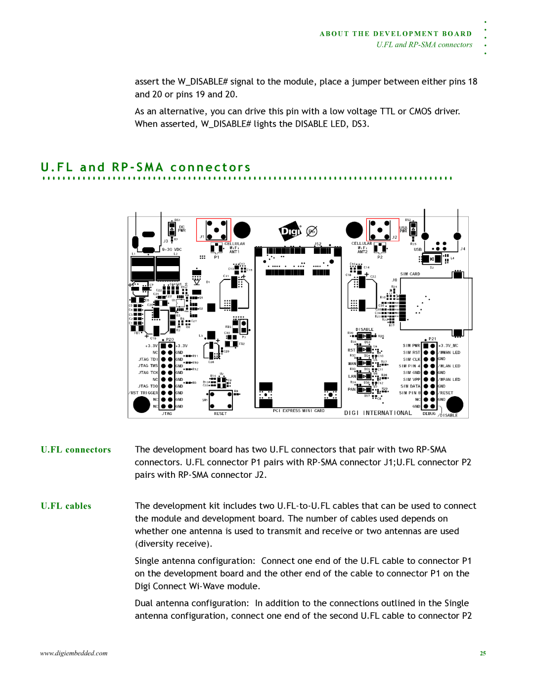
U.FL connectors | The development board has two U.FL connectors that pair with two |
| connectors. U.FL connector P1 pairs with |
| pairs with |
U.FL cables | The development kit includes two |
| the module and development board. The number of cables used depends on |
| whether one antenna is used to transmit and receive or two antennas are used |
| (diversity receive). |
| Single antenna configuration: Connect one end of the U.FL cable to connector P1 |
| on the development board and the other end of the cable to connector P1 on the |
| Digi Connect |
| Dual antenna configuration: In addition to the connections outlined in the Single |
| antenna configuration, connect one end of the second U.FL cable to connector P2 |
www.digiembedded.com | 25 |
