MB3788
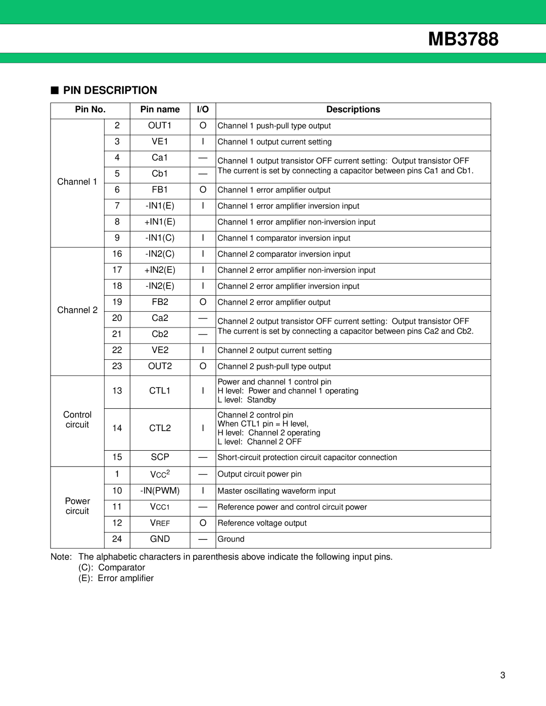
■PIN DESCRIPTION
Pin No. |
| Pin name | I/O | Descriptions | |
|
|
|
|
|
|
|
| 2 | OUT1 | O | Channel 1 |
|
|
|
|
|
|
|
| 3 | VE1 | I | Channel 1 output current setting |
|
|
|
|
|
|
|
| 4 | Ca1 | — | Channel 1 output transistor OFF current setting: Output transistor OFF |
|
|
|
|
| |
|
|
|
|
| The current is set by connecting a capacitor between pins Ca1 and Cb1. |
Channel 1 |
| 5 | Cb1 | — | |
|
| ||||
|
|
|
|
| |
| 6 | FB1 | O | Channel 1 error amplifier output | |
|
| ||||
|
|
|
|
|
|
|
| 7 | I | Channel 1 error amplifier inversion input | |
|
|
|
|
|
|
|
| 8 | +IN1(E) |
| Channel 1 error amplifier |
|
|
|
|
|
|
|
| 9 | I | Channel 1 comparator inversion input | |
|
|
|
|
|
|
|
| 16 | I | Channel 2 comparator inversion input | |
|
|
|
|
|
|
|
| 17 | +IN2(E) | I | Channel 2 error amplifier |
|
|
|
|
|
|
|
| 18 | I | Channel 2 error amplifier inversion input | |
|
|
|
|
|
|
Channel 2 |
| 19 | FB2 | O | Channel 2 error amplifier output |
|
|
|
|
| |
| 20 | Ca2 | — | Channel 2 output transistor OFF current setting: Output transistor OFF | |
|
| ||||
|
|
|
|
| |
|
|
|
|
| The current is set by connecting a capacitor between pins Ca2 and Cb2. |
|
| 21 | Cb2 | — | |
|
|
| |||
|
|
|
|
|
|
|
| 22 | VE2 | I | Channel 2 output current setting |
|
|
|
|
|
|
|
| 23 | OUT2 | O | Channel 2 |
|
|
|
|
|
|
|
| 13 | CTL1 | I | Power and channel 1 control pin |
|
| H level: Power and channel 1 operating | |||
|
|
|
|
| L level: Standby |
Control |
|
|
|
|
|
|
|
|
| Channel 2 control pin | |
circuit |
| 14 | CTL2 | I | When CTL1 pin = H level, |
|
| H level: Channel 2 operating | |||
|
|
|
|
| |
|
|
|
|
| L level: Channel 2 OFF |
|
|
|
|
|
|
|
| 15 | SCP | — | |
|
|
|
|
|
|
|
| 1 | VCC2 | — | Output circuit power pin |
|
|
|
|
|
|
|
| 10 |
| I | Master oscillating waveform input |
Power |
|
|
|
|
|
| 11 | VCC1 | — | Reference power and control circuit power | |
circuit |
| ||||
|
|
|
|
| |
|
| 12 | VREF | O | Reference voltage output |
|
|
|
|
|
|
|
| 24 | GND | — | Ground |
|
|
|
|
|
|
Note: The alphabetic characters in parenthesis above indicate the following input pins. (C): Comparator
(E): Error amplifier
3