|
|
|
|
|
|
|
|
|
|
|
|
| AUTOMOTIVE 80C51FA/83C51FA | |||||||
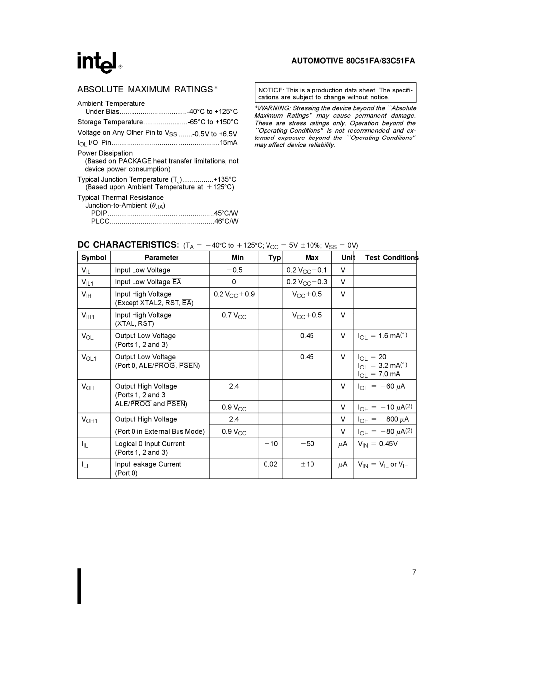
ABSOLUTE MAXIMUM RATINGS* |
|
|
|
|
|
| ||||||||||||||
NOTICE: This is a production data sheet. The specifi- |
| |||||||||||||||||||
Ambient Temperature |
|
|
|
| cations are subject to change without notice. |
| ||||||||||||||
|
|
|
| *WARNING: Stressing the device beyond the ``Absolute | ||||||||||||||||
Under Bias | ||||||||||||||||||||
Maximum Ratings'' may cause permanent damage. | ||||||||||||||||||||
Storage Temperature |
| |||||||||||||||||||
These are stress ratings only. Operation beyond the | ||||||||||||||||||||
Voltage on Any Other Pin to VSS | ``Operating Conditions'' is not recommended and ex- | |||||||||||||||||||
IOL I/O Pin | ........................................................ |
|
|
|
|
|
|
| 15mA | tended exposure beyond the ``Operating Conditions'' | ||||||||||
|
|
|
|
|
|
|
|
| may affect device reliability. |
|
|
|
|
| ||||||
Power Dissipation |
|
|
|
|
|
|
|
|
|
|
|
|
| |||||||
(Based on PACKAGE heat transfer limitations, not |
|
|
|
|
|
|
|
|
| |||||||||||
device power consumption) |
|
|
|
|
|
|
|
|
|
|
|
|
| |||||||
Typical Junction Temperature (TJ) |
|
| +135°C |
|
|
|
|
|
|
|
|
| ||||||||
(Based upon Ambient Temperature at a125§C) |
|
|
|
|
|
|
|
|
| |||||||||||
Typical Thermal Resistance |
|
|
|
|
|
|
|
|
|
|
|
|
| |||||||
|
| 45°C/W |
|
|
|
|
|
|
|
|
| |||||||||
PDIP |
|
|
|
|
|
|
|
|
|
|
|
|
|
|
|
|
|
| ||
PLCC |
|
|
|
|
|
|
|
| 46°C/W |
|
|
|
|
|
|
|
|
| ||
DC CHARACTERISTICS: (TA e b40§C to a125§C; VCC e 5V g10%; VSS e 0V) |
|
| ||||||||||||||||||
Symbol | Parameter |
|
|
| Min |
| Typ | Max |
| Unit |
| Test Conditions |
| |||||||
VIL | Input Low Voltage |
|
|
| b0.5 |
|
| 0.2 VCCb0.1 |
| V |
|
|
|
| ||||||
VIL1 | Input Low Voltage |
|
|
|
|
|
|
| 0 |
|
| 0.2 VCCb0.3 |
| V |
|
|
|
| ||
EA |
|
|
|
|
|
|
|
| ||||||||||||
VIH | Input High Voltage |
|
|
| 0.2 VCCa0.9 |
| VCCa0.5 |
| V |
|
|
|
| |||||||
| (Except XTAL2, RST, | EA) |
|
|
|
|
|
|
|
|
|
|
|
| ||||||
VIH1 | Input High Voltage |
|
|
| 0.7 VCC |
|
| VCCa0.5 |
| V |
|
|
|
| ||||||
| (XTAL, RST) |
|
|
|
|
|
|
|
|
|
|
|
|
| ||||||
V | Output Low Voltage |
|
|
|
|
|
| 0.45 |
| V |
| I | e 1.6 mA(1) |
| ||||||
OL | (Ports 1, 2 and 3) |
|
|
|
|
|
|
|
|
|
| OL |
|
| ||||||
|
|
|
|
|
|
|
|
|
|
|
|
|
| |||||||
VOL1 | Output Low Voltage |
|
|
|
|
|
| 0.45 |
| V |
| IOL e 20 |
| |||||||
| (Port 0, ALE/PROG , | PSEN) |
|
|
|
|
|
|
|
| I | e 3.2 mA(1) |
| |||||||
|
|
|
|
|
|
|
|
|
|
|
|
|
|
|
|
| OL |
|
| |
|
|
|
|
|
|
|
|
|
|
|
|
|
|
|
|
| IOL e 7.0 mA |
| ||
VOH | Output High Voltage |
|
|
| 2.4 |
|
|
|
| V |
| IOH e b60 mA |
| |||||||
| (Ports 1, 2 and 3 |
|
|
|
|
|
|
|
|
|
|
|
|
| ||||||
| ALE/PROG and | PSEN) |
| 0.9 V |
|
|
|
| V |
| I | e b10 mA(2) |
| |||||||
|
|
|
|
|
|
|
|
|
| CC |
|
|
|
|
|
| OH |
|
| |
VOH1 | Output High Voltage |
|
|
| 2.4 |
|
|
|
| V |
| IOH e b800 mA |
| |||||||
| (Port 0 in External Bus Mode) | 0.9 V |
|
|
|
| V |
| I | e b80 mA(2) |
| |||||||||
|
|
|
|
|
|
|
|
|
| CC |
|
|
|
|
|
| OH |
|
| |
IIL | Logical 0 Input Current |
|
|
|
|
| b10 | b50 |
| mA |
| VIN e 0.45V |
| |||||||
| (Ports 1, 2 and 3) |
|
|
|
|
|
|
|
|
|
|
|
|
| ||||||
ILI | Input leakage Current |
|
|
|
|
| 0.02 | g10 |
| mA |
| VIN e VIL or VIH |
| |||||||
| (Port 0) |
|
|
|
|
|
|
|
|
|
|
|
|
| ||||||
7