addresses (MOVX @Ri), Port 2 emits the contents of the P2 Special Function Register.
Port 3: Port 3 is an
Port 3 also serves the functions of various special features of the MCS 51 microcontroller family, as listed below:
Port Pin | Alternate Function |
P3.0 | RXD (serial input port) |
P3.1 | TXD (serial output port) |
P3.2 | INT0 (external interrupt 0) |
P3.3 | INT1 (external interrupt 1) |
P3.4 | T0 (Timer 0 external input) |
P3.5 | T1 (Timer 1 external input) |
P3.6 | WR (external data memory write strobe) |
P3.7 | RD (external data memory read strobe) |
RESET: Reset input. A high on this pin for two ma- chine cycles while the oscillator is running resets the device. An internal pulldown resistor permits a pow-
ALE/PROG : Address Latch Enable output pulse for latching the low byte of the address during accesses to external memory.
In normal operation ALE is emitted at a constant rate of (/6 the oscillator frequency, and may be used for external timing or clocking purposes. Note, how- ever, that one ALE pulse is skipped during each ac- cess to external Data Memory.
Throughout the remainder of this datasheet, ALE will refer to the signal coming out of the ALE/PROG pin, and the pin will be referred to as the ALE/PROG pin.
PSEN: Program Store Enable is the read strobe to external Program Memory.
When the 83C51FA is executing code from external Program Memory, PSEN is activated twice each ma- chine cycle, except that two PSEN activations are skipped during each access to external Data Memo- ry.
AUTOMOTIVE 80C51FA/83C51FA
EA/V PP: External Access enable. EA must be strapped to VSS in order to enable the device to fetch code from external Program Memory locations 0000H to 0FFFFH. Note, however, that if either of the Program Lock bits are programmed, EA will be internally latched on reset.
EA should be strapped to VCC for internal program executions.
XTAL1: Input to the inverting oscillator amplifier.
XTAL2: Output from the inverting oscillator amplifi- er.
OSCILLATOR CHARACTERISTICS
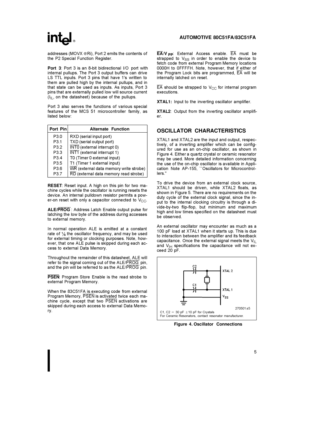
XTAL1 and XTAL2 are the input and output, respec- tively, of a inverting amplifier which can be config- ured for use as an
To drive the device from an external clock source, XTAL1 should be driven, while XTAL2 floats, as shown in Figure 5. There are no requirements on the duty cycle of the external clock signal, since the in- put to the internal clocking circuitry is through a di-
An external oscillator may encounter as much as a 100 pF load at XTAL1 when it starts up. This is due to interaction between the amplifier and its feedback capacitance. Once the external signal meets the VIL and VIH specifications the capacitance will not ex- ceed 20 pF.
270501 ±5
C1, C2 e 30 pF g10 pF for Crystals
For Ceramic Resonators, contact resonator manufacturer.
Figure 4. Oscillator Connections
5