Evaluation Board for Quad T1/E1 Applications — LXD386
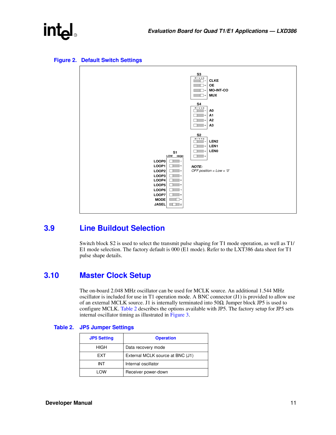
Figure 2. Default Switch Settings
|
| S1 | |
| LOW HIGH | ||
LOOP0 |
|
| 1 |
|
|
| |
S3
FFO ![]()
![]() 1
1
2
3
4
S4
FFO ![]()
![]() 1
1
2
3
4
S2
FFO ![]()
![]() 1
1
2
3
4
CLKE OE
A0
A1
A2
A3
LEN2
LEN1
LEN0
LOOP1 |
|
| 2 | |
|
|
| ||
LOOP2 |
|
| 3 | |
|
|
| ||
LOOP3 |
|
| ||
|
| 4 | ||
|
|
| ||
LOOP4 |
|
| ||
|
| 5 | ||
LOOP5 |
|
| ||
|
| 6 | ||
LOOP6 |
|
|
| |
|
| 7 | ||
|
|
| ||
LOOP7 |
|
| ||
|
| 8 | ||
|
|
| ||
MODE |
|
|
| |
|
|
| 9 | |
|
|
|
| |
JASEL |
|
|
| |
|
|
| 10 | |
NOTE:
OFF position = Low = ’0’
3.9Line Buildout Selection
Switch block S2 is used to select the transmit pulse shaping for T1 mode operation, as well as T1/ E1 mode selection. The factory default is 000 (E1 mode). Refer to the LXT386 data sheet for T1 pulse shape details.
3.10Master Clock Setup
The
Table 2. JP5 Jumper Settings
JP5 Setting | Operation |
|
|
HIGH | Data recovery mode |
|
|
EXT | External MCLK source at BNC (J1) |
|
|
INT | Internal oscillator |
|
|
LOW | Receiver |
|
|
Developer Manual | 11 |