Intel® LXD972M Transceiver Demo Board (Board Rev A1)
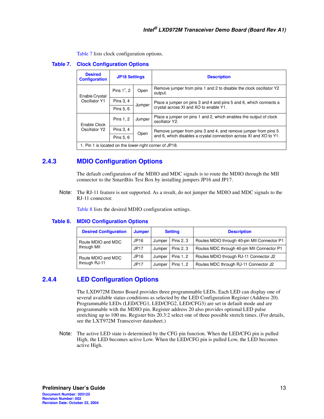
Table 7 lists clock configuration options.
Table 7. Clock Configuration Options
Desired | JP18 Settings | Description | ||
Configuration | ||||
|
|
| ||
|
|
|
| |
| Pins 11, 2 | Open | Remove jumper from pins 1 and 2 to disable the clock oscillator Y2 | |
Enable Crystal |
|
| output. | |
|
|
| ||
Oscillator Y1 | Pins 3, 4 | Jumper | Place a jumper on pins 3 and 4 and pins 5 and 6, which connects a | |
|
| |||
| Pins 5, 6 | crystal across XI and XO to enable Y1. | ||
|
| |||
|
|
| ||
|
|
|
| |
| Pins 1, 2 | Jumper | Place a jumper on pins 1 and 2, which enables the output of clock | |
Enable Clock |
|
| oscillator Y2. | |
|
|
| ||
Oscillator Y2 | Pins 3, 4 | Open | Remove jumper from pins 3 and 4, and remove jumper from pins 5 | |
|
| |||
| Pins 5, 6 | and 6, which disables a crystal connection across XI and XO to Y1. | ||
|
| |||
|
|
| ||
|
|
|
| |
1. Pin 1 is located on the | ||||
|
|
|
| |
2.4.3MDIO Configuration Options
The default configuration of the MDIO and MDC signals is to route the MDIO through the MII connector to the SmartBits Test Box by installing jumpers JP16 and JP17.
Note: The
Table 8 lists the desired MDIO configuration settings.
Table 8. MDIO Configuration Options
Desired Configuration | Jumper | Setting | Description | |
|
|
|
|
|
Route MDIO and MDC | JP16 | Jumper | Pins 2, 3 | Routes MDIO through |
|
|
|
| |
through MII | JP17 | Jumper | Pins 2, 3 | Routes MDC through |
| ||||
|
|
|
|
|
Route MDIO and MDC | JP16 | Jumper | Pins 1, 2 | Routes MDIO through |
|
|
|
| |
through | JP17 | Jumper | Pins 1, 2 | Routes MDC through |
| ||||
|
|
|
|
|
2.4.4LED Configuration Options
The LXD972M Demo Board provides three programmable LEDs. Each LED can display one of several available status conditions as selected by the LED Configuration Register (Address 20). Programmable LEDs (LED/CFG1, LED/CFG2, LED/CFG3) are set in default mode and are programmable with the MDIO pin. Register address 20 also provides optional LED pulse stretching up to 100 ms. Register bits 20.3:2 select one of three possible stretch times. (For details, see the LXT972M Transceiver datasheet.)
Note: The active LED state is determined by the CFG pin function. When the LED/CFG pin is pulled High, the LED becomes active Low. When the LED/CFG pin is pulled Low, the LED becomes active High.
Preliminary User’s Guide | 13 |
Document Number: 303125
Revision Number: 002
Revision Date: October 22, 2004
