Intel® LXD972M Transceiver Demo Board (Board Rev A1)
2.4.2Power Supply Voltage Source and Clock Options
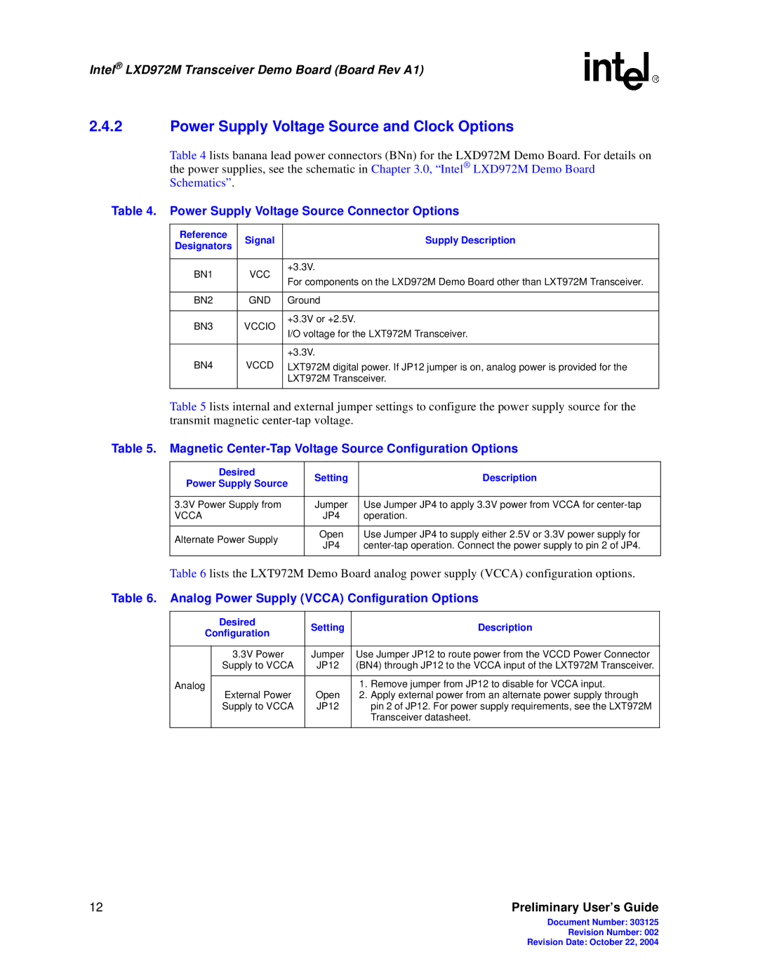
Table 4 lists banana lead power connectors (BNn) for the LXD972M Demo Board. For details on the power supplies, see the schematic in Chapter 3.0, “Intel® LXD972M Demo Board Schematics”.
Table 4. Power Supply Voltage Source Connector Options
Reference | Signal | Supply Description | |
Designators | |||
|
| ||
|
|
| |
BN1 | VCC | +3.3V. | |
For components on the LXD972M Demo Board other than LXT972M Transceiver. | |||
|
| ||
|
|
| |
BN2 | GND | Ground | |
|
|
| |
BN3 | VCCIO | +3.3V or +2.5V. | |
I/O voltage for the LXT972M Transceiver. | |||
|
| ||
|
|
| |
|
| +3.3V. | |
BN4 | VCCD | LXT972M digital power. If JP12 jumper is on, analog power is provided for the | |
|
| LXT972M Transceiver. | |
|
|
|
Table 5 lists internal and external jumper settings to configure the power supply source for the transmit magnetic
Table 5. Magnetic Center-Tap Voltage Source Configuration Options
Desired | Setting | Description | |
Power Supply Source | |||
|
| ||
|
|
| |
3.3V Power Supply from | Jumper | Use Jumper JP4 to apply 3.3V power from VCCA for | |
VCCA | JP4 | operation. | |
|
|
| |
Alternate Power Supply | Open | Use Jumper JP4 to supply either 2.5V or 3.3V power supply for | |
JP4 | |||
| |||
|
|
|
Table 6 lists the LXT972M Demo Board analog power supply (VCCA) configuration options.
Table 6. Analog Power Supply (VCCA) Configuration Options
| Desired | Setting |
| Description |
Configuration |
| |||
|
|
| ||
|
|
|
| |
| 3.3V Power | Jumper | Use Jumper JP12 to route power from the VCCD Power Connector | |
| Supply to VCCA | JP12 | (BN4) through JP12 to the VCCA input of the LXT972M Transceiver. | |
|
|
|
|
|
Analog | External Power | Open | 1. | Remove jumper from JP12 to disable for VCCA input. |
| 2. | Apply external power from an alternate power supply through | ||
| Supply to VCCA | JP12 |
| pin 2 of JP12. For power supply requirements, see the LXT972M |
|
|
|
| Transceiver datasheet. |
|
|
|
|
|
12 | Preliminary User’s Guide |
Document Number: 303125
Revision Number: 002
Revision Date: October 22, 2004