Introduction
1.Introduction
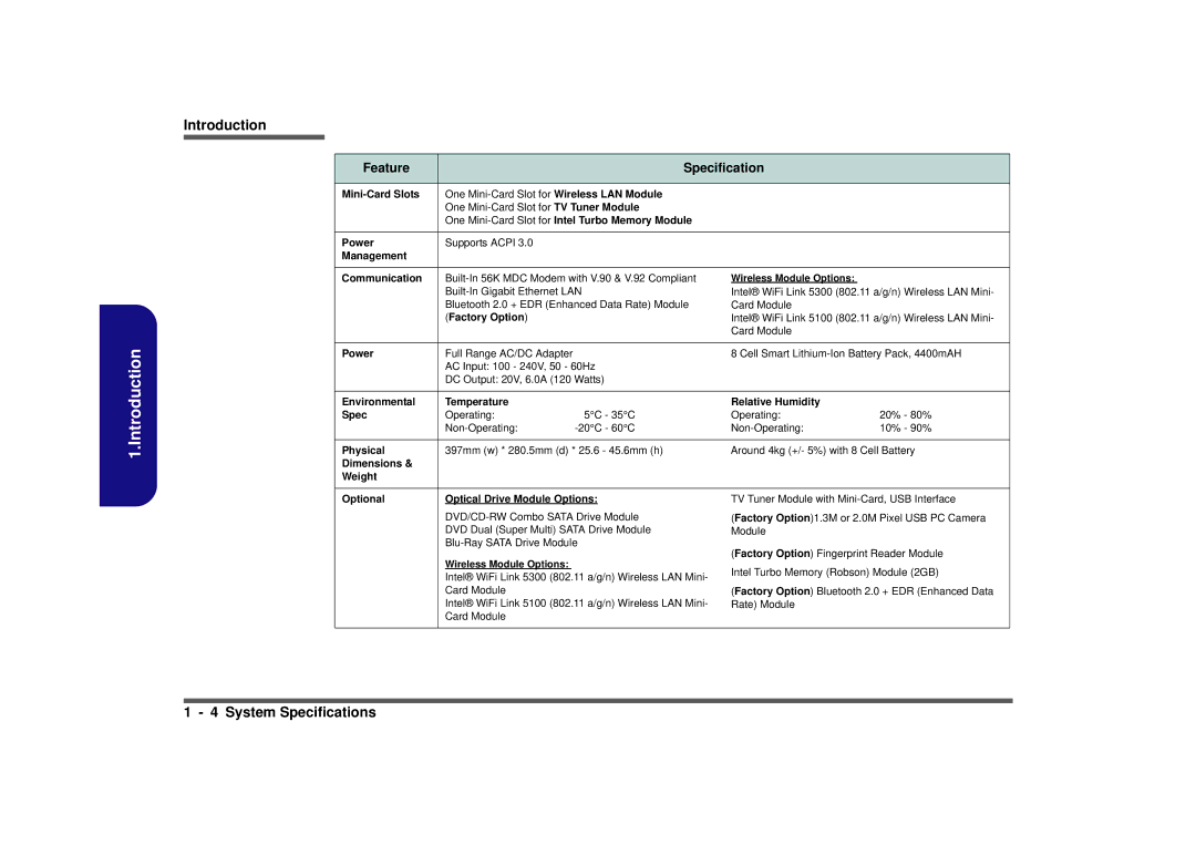
Feature |
| Specification |
| |
|
|
|
| |
| One |
|
| |
| One |
|
| |
| One |
|
| |
|
|
|
|
|
Power | Supports ACPI 3.0 |
|
|
|
Management |
|
|
|
|
|
|
|
| |
Communication | Wireless Module Options: |
| ||
| Intel® WiFi Link 5300 (802.11 a/g/n) Wireless LAN Mini- | |||
| Bluetooth 2.0 + EDR (Enhanced Data Rate) Module | Card Module |
| |
| (Factory Option) |
| Intel® WiFi Link 5100 (802.11 a/g/n) Wireless LAN Mini- | |
|
|
| Card Module |
|
|
|
|
| |
Power | Full Range AC/DC Adapter |
| 8 Cell Smart | |
| AC Input: 100 - 240V, 50 - 60Hz |
|
| |
| DC Output: 20V, 6.0A (120 Watts) |
|
| |
|
|
|
|
|
Environmental | Temperature |
| Relative Humidity |
|
Spec | Operating: | 5°C - 35°C | Operating: | 20% - 80% |
| 10% - 90% | |||
|
|
| ||
Physical | 397mm (w) * 280.5mm (d) * 25.6 - 45.6mm (h) | Around 4kg (+/- 5%) with 8 Cell Battery | ||
Dimensions & |
|
|
|
|
Weight |
|
|
|
|
|
|
| ||
Optional | Optical Drive Module Options: | TV Tuner Module with | ||
| (Factory Option)1.3M or 2.0M Pixel USB PC Camera | |||
| DVD Dual (Super Multi) SATA Drive Module | Module |
| |
| (Factory Option) Fingerprint Reader Module | |||
| Wireless Module Options: |
| ||
|
| Intel Turbo Memory (Robson) Module (2GB) | ||
| Intel® WiFi Link 5300 (802.11 a/g/n) Wireless LAN Mini- | |||
|
|
| ||
| Card Module |
| (Factory Option) Bluetooth 2.0 + EDR (Enhanced Data | |
| Intel® WiFi Link 5100 (802.11 a/g/n) Wireless LAN Mini- | Rate) Module |
| |
| Card Module |
|
|
|
|
|
|
|
|