Page
Page
M570TU
Trademarks
About this Manual
Important Safety Instructions
FCC Statement
FCC RF Radiation Exposure Statement
Instructions for Care and Operation
Power Safety
Battery Precautions
Related Documents
Contents
XII
Introduction
Feature Specification
System Specifications
System Specifications 1
Mini-Card Slots
Top View
External Locator Top View with LCD Panel Open
Overheating
External Locator Front & Rear View
Right & Left Side View
External Locator Right & Left Side View
Bottom View
External Locator Bottom View
Mainboard Top Key Parts
Mainboard Overview Top Key Parts
Mainboard Bottom Key Parts
Mainboard Overview Bottom Key Parts
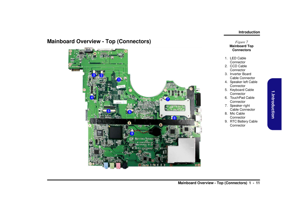
Mainboard Top Connectors
Mainboard Overview Top Connectors
Mainboard Bottom Connectors
Mainboard Overview Bottom Connectors
Overview
Disassembly
Disassembly
Maintenance Precautions
To remove the VGA Card To remove the Modem
Disassembly Steps
To remove the Inverter Board
Battery Removal
Removing the Battery
Removing the Hard Disk Drive
HDD Assembly Removal
HDD Assembly Removal cont’d
Optical Device Removal
Removing the Optical CD/DVD Device
RAM Module Removal
Removing the System Memory RAM
Processor Removal
Removing and Installing the Processor
Unlock
Processor Removal Cont’d
Remove the sticker
Processor Installation
VGA Card Removal
Removing the VGA Card
Wireless LAN Module Removal
Removing the Wireless LAN Module
TV Tuner Card Removal
Removing the TV Tuner Card
Turbo Memory Card Removal
Removing the Turbo Memory Card
Bluetooth Module Removal
Removing the Bluetooth Module
Keyboard Removal
Removing the Keyboard
Modem Removal
Removing the Modem
Modem Removal cont’d
Inverter Board Removal
Removing the Inverter Board
Appendix APart Lists
Part List Illustration Location
Part List Illustration Location
Top with Finger Print
Top with Fingerprint
Top without Fingerprint
Top without Fingerprint
Bottom
LCD
DVD Combo Drive
DVD Combo Drive
DVD Super-Multi Drive
DVD Super-Multi Drive
Schematic Diagrams
Appendix BSchematic Diagrams
Sheet 1
System Block Diagram
Sheet 2 Penryn 1/2
Penryn 1/2
TH E R MD a
TH E R MD C
Sheet 3 Penryn 2/2
Penryn 2/2
LE R T
A T a
Sheet 4 Cantiga 1/5 Host
Cantiga 1/5 Host
N T I G a
Sheet 5 Crestline 2/6 PEG
Cantiga 2/6 PEG
R C O MP
LK D R E F
Sheet 6 Crestline 3/6 DDR
Cantiga 3/6 DDR
Sheet 7 Crestline 4/6
Crestline 4/6 POWER1
Sheet 8 Cantiga 5/6 GND
Cantiga 5/6 GND
9 1
GP LL
1 0 , 11 , 2 8 , 3 1 1
4 , 1 3 , 16 , 2 3 , 3 2 1 5V S
Sheet 10
DDR3 SO-DIMM
D S P D
T E S T
Sheet 11
Sheet 12
LCD,CPU FAN
Sheet 13
ICH9-M 1/4 Sata
Sheet 14
ICH9-M 2/4 PCI,USB
Sheet 15
Sheet 16 ICH9-M 4/4
ICH9-M 4/4
C0 USB
Sheet 17 ODD, PC BEEP, USB2.0 & eSATA
OU T
GN D4
Sheet 18
Clock GENERATOR, CCD
Sheet 19
PCI-E LAN RTL8111C
RTL8111C
C S
Sheet 20
Card Reader & 1394 JMB380
1394 JMB380
Sheet 21
NEW Card
Sheet 22 of 42 KBC-ITE IT8512
KBC-ITE IT8512
I G H T N E S S
TP C L K
Sheet 23
Hdmi
MI C LK
4 1 LE D B a T C H G #
Sheet 24
E D B a T F U L L #
3 6 W L a N E N
D I F -OU T
Azalia Codec ALC662
GH OU T
JH E a D P H on E -R
SPKOUTR+
MUTEAPM#
Spkoutr Muteapm
SPKOUTL+ Spkoutl H822 KBCMUTE#
Sheet 27
SRS
Alazia MDC
CRT, INV, MDC, BT, Pwrgd
T CO N
Sheet 29 Power Charger, DC
I N
E F
Sheet 30 Power GPU
Power GPU
RA M P
GS S
Sheet 31 Power 1.5V
Power 1.5V
GO OD
Power 1.8VS/ 1.05VS
Sheet 33 Power 3VS, 5VS Power S/W
Power 3VS, 5VS, Power S/W
Sheet 34 Power VDD3 VDD5/ 3.3V
Power VDD3/ VDD5/ 3.3V
S B L
LD O5
C S E N S E
Sheet 35 Power Vcore for Penryn CPU
S S E N S E
R S L
Sheet 36
Mini CARD, CIR
Sheet 37
MXM PCI-E TYPE-IV
Sheet 38 Board to board
Board to board CON
GCON1
Sheet 39
Button Board
Sheet 40 of 42 Click Board
Click Board
Sheet 41 Fingerprint Board
Fingerprint Board
Ledr *LEDR
Debug Board
CLR GND QH
80CL K- FH
Schematic Diagrams