IDE Interface Connector
All signal levels in the IDE interface are TTL compatible. A logic 1 is a signal whose voltage level is between 2.0 and 5.0 V. A logic 0 is a signal measuring between 0.00 and 0.70 V.
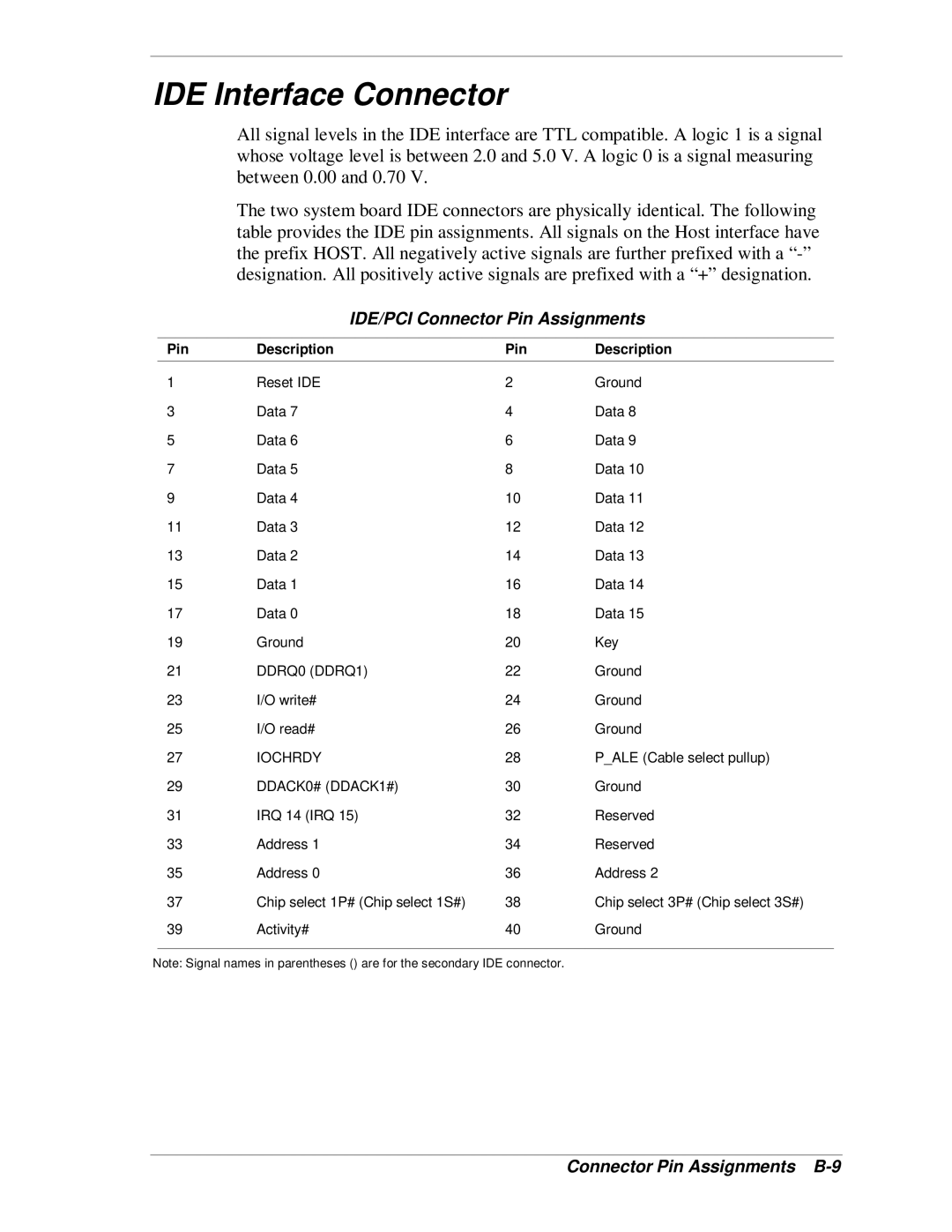
The two system board IDE connectors are physically identical. The following table provides the IDE pin assignments. All signals on the Host interface have the prefix HOST. All negatively active signals are further prefixed with a
IDE/PCI Connector Pin Assignments
Pin | Description | Pin | Description |
1 | Reset IDE | 2 | Ground |
3 | Data 7 | 4 | Data 8 |
5 | Data 6 | 6 | Data 9 |
7 | Data 5 | 8 | Data 10 |
9 | Data 4 | 10 | Data 11 |
11 | Data 3 | 12 | Data 12 |
13 | Data 2 | 14 | Data 13 |
15 | Data 1 | 16 | Data 14 |
17 | Data 0 | 18 | Data 15 |
19 | Ground | 20 | Key |
21 | DDRQ0 (DDRQ1) | 22 | Ground |
23 | I/O write# | 24 | Ground |
25 | I/O read# | 26 | Ground |
27 | IOCHRDY | 28 | P_ALE (Cable select pullup) |
29 | DDACK0# (DDACK1#) | 30 | Ground |
31 | IRQ 14 (IRQ 15) | 32 | Reserved |
33 | Address 1 | 34 | Reserved |
35 | Address 0 | 36 | Address 2 |
37 | Chip select 1P# (Chip select 1S#) | 38 | Chip select 3P# (Chip select 3S#) |
39 | Activity# | 40 | Ground |
Note: Signal names in parentheses () are for the secondary IDE connector.