TS-440S

CIRCUIT DESCRIPTION

VCO I A 45 .08. . 52 .55 MHz

852 .55 ... 59 .55 MH z C 59 .55 . . 67 .05MH z D 67.05 ., . 75 .05MHz

25C266B


2502668

VCO


I

36 .22MHZ

037

03 8


I


D


55A5


Co


vco


FM MO D


HET


4508.- .]5G5MH=.


LO


2561924


25C266B


(OCT I


Q25


1 8 375MH z


Q3 6

15KHZ1

20KHZ : FM I


Q26


BUFF


I


A .LPF

o 3l , 32 , 3 3


LfLO --- -


2SC2668


J


6 14 7


CA R


2502459 x 3


2SC2458


SFT


} 500KHz

PLL


ICI4

8.5539 .05 MH z


2502459 . 2

IC18


CAR


II


P .

_ 9MH x


IC1 2


024

IC 13


034,3 5


PHA . C .

1017


SN169138


BUFF

Di v

9MHz


7244 9MHz

Q 6

250245 8


3-]3


6.5-.36 .5MH

SN15913 P


1 i


30.175-30.675M H


4


118111 FM )


AMR,FMR : O N


DIV

SN74SII2N

IC1 6


2502668

SN7RS,12 N


AMT , FM T


/456 .5KHZ USB,CW

1


1/30,1/2

SN74SION

IC1 5


r ST D


1453 .5KHZ LSB,FSK


4

030

029

Q27,2 8

5.82 5

5 32 5


02 3

Q22

6


I C 3

455KHZ

Q 7

`\

AMR,FM R


\


BUF F

BUFF

ST D

Q2 1


®

2502458to-


OSC


2SC2668

2502668


2S 0266822


SNI6913F 250266 8

2SC266 8

250278 7


SN 74LS9 0

250195 9


IC1I

IC10


020

IC8

6 .53-.6 .63MHZ 10 7

0 9

4 .55MH z

54460L

2SC2668

0SN16913 P

BPF

O

UFF

LPF


SN16913P 2502458

58 .25-53 .25MHz

Q1 8

111019

64 .78-59 .88MHz 1 .98-2 .08M4z

IC 6

IC 5


B P F


LPF

/

DI V


5

I/1 0


2502668 2SC266 8


SN74LS90N M54460L

016,17

I20KHZI IC9

015


-IO 4

A LPF h-1

P . D

B .A P


99 .

I 'PHA . C .


Q12

2503113 x 2

S 1 R MN6147 2802668


2502668®


M 9MHz


010,11


3239.. 2994 (STEP 51


A . LPF


2503113 . 2

IC 2

0 5


AM,F M


91MHZ /91 .3MHZ . USB 4 O w

5

459 L

2SC2668


2SC266 8

2SC2668 90.7MHZ : LSH.FS K


PL L 4


15K Hz (

01 4


P D

01, 2

BUFF

MN6147


C

I

25031132 2


2SC266 8


9MHz K 18200


01 3


I/ 18260

: USB , C w


\18140 LS8,FS K


250266 6

IPLL 3


IF SHIFT I-40--401


CAR

I-16-. 15 )

(5K H


P D

_ IC 4


HA C

MN 614 7


L 9MHz

RITZ-120- ,120 1


19800- 2079 9


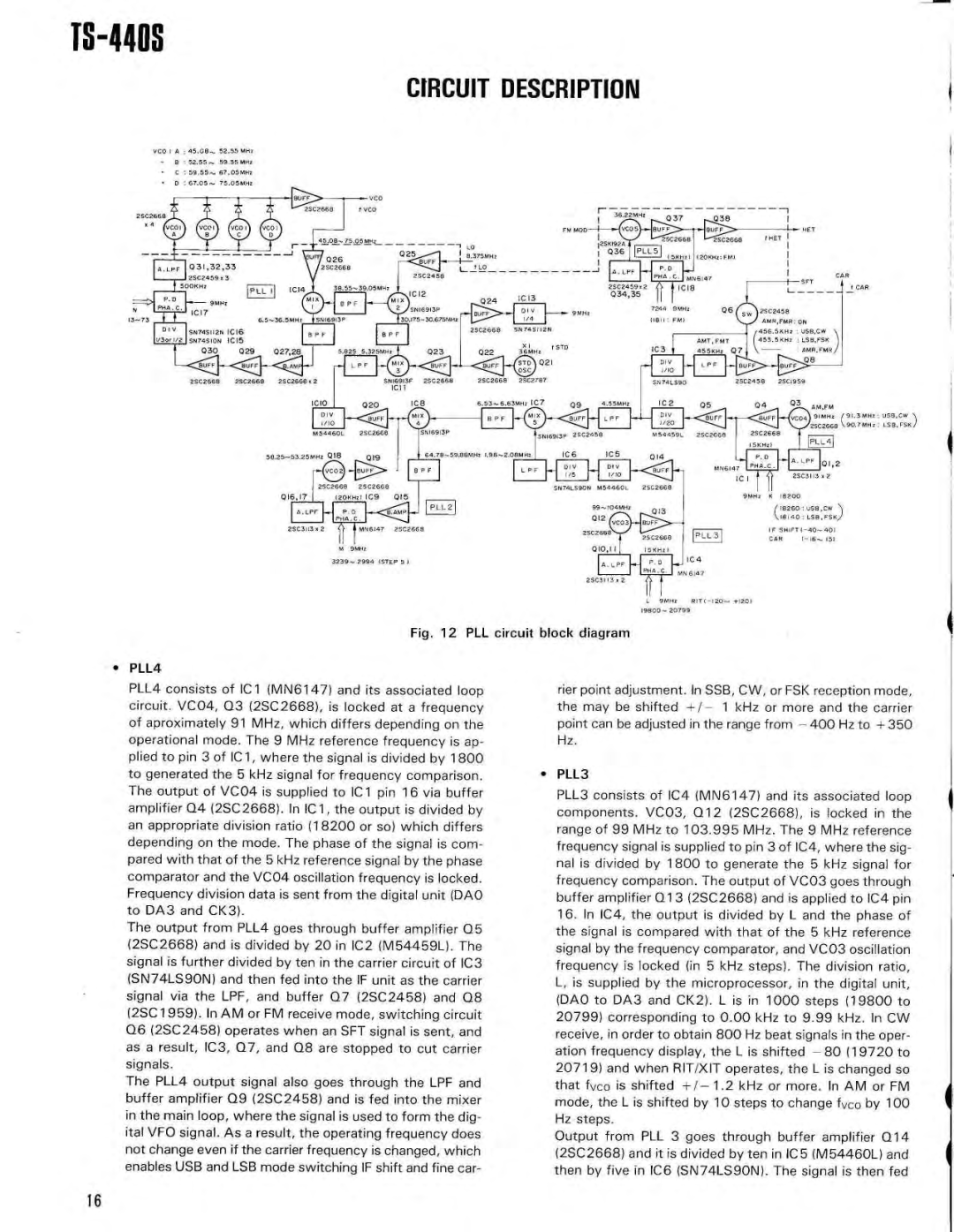
Fig . 12 PLL circuit block diagra m

PLL4

PLL4 consists of IC1 (MN6147) and its associated loo p circuit . VC04, Q3 (2SC2668), is locked at a frequenc y of aproximately 91 MHz, which differs depending on th e operational mode . The 9 MHz reference frequency is ap- plied to pin 3 of ICI, where the signal is divided by 180 0 to generated the 5 kHz signal for frequency comparison . The output of VC04 is supplied to IC1 pin 16 via buffe r amplifier Q4 (2SC2668) . In ICI, the output is divided b y an appropriate division ratio (18200 or so) which differ s depending on the mode . The phase of the signal is com- pared with that of the 5 kHz reference signal by the phas e comparator and the VC04 oscillation frequency is locked . Frequency division data is sent from the digital unit (DA O to DA3 and CK3) .

The output from PLL4 goes through buffer amplifier Q 5 (2SC2668) and is divided by 20 in IC2 (M54459L( . Th e signal is further divided by ten in the carrier circuit of IC 3 (SN74LS90N) and then fed into the IF unit as the carrie r signal via the LPF, and buffer Q7 (2SC2458) and Q 8 (2SC 1959) . In AM or FM receive mode, switching circui t Q6 (2SC2458) operates when an SFT signal is sent, an d as a result, IC3, Q7, and Q8 are stopped to cut carrie r signals .

The PLL4 output signal also goes through the LPF an d buffer amplifier Q9 (2SC2458) and is fed into the mixe r in the main loop, where the signal is used to form the dig - ital VFO signal . As a result, the operating frequency doe s not change even if the carrier frequency is changed, whic h enables USB and LSB mode switching IF shift and fine car -

rier point adjustment . In SSB, CW, or FSK reception mode , the may be shifted +/– 1 kHz or more and the carrie r point can be adjusted in the range from – 400 Hz to + 35 0 Hz .

PLL3

PLL3 consists of IC4 (MN6147) and its associated loo p components . VCO3, Q12 (2SC2668), is locked in th e range of 99 MHz to 103 .995 MHz . The 9 MHz referenc e frequency signal is supplied to pin 3 of IC4, where the sig - nal is divided by 1800 to generate the 5 kHz signal fo r frequency comparison . The output of VCO3 goes throug h buffer amplifier Q13 (2SC2668) and is applied to IC4 pi n 16 . In IC4, the output is divided by L and the phase o f the signal is compared with that of the 5 kHz referenc e signal by the frequency comparator, and VCO3 oscillatio n frequency is locked (in 5 kHz steps) . The division ratio , L, is supplied by the microprocessor, in the digital unit , (DAO to DA3 and CK2) . L is in 1000 steps (19800 t o 20799) corresponding to 0 .00 kHz to 9 .99 kHz . In C W receive, in order to obtain 800 Hz beat signals in the oper - ation frequency display, the L is shifted -80 (19720 t o 20719) and when RIT/XIT operates, the Lis changed s o that fvco is shifted +1– 1 .2 kHz or more . In AM or F M mode, the L is shifted by 10 steps to change fvco by 10 0 Hz steps .

Output from PLL 3 goes through buffer amplifier Q1 4 (2SC2668) and it is divided by ten in IC5 (M54460L) an d then by five in IC6 (SN74LS90N) . The signal is then fe d

16

Page 16
Image 16
Kenwood PS-50, SP-430, PS-430, MB-430, AT-440, VS-1, YK-88SN, YK-88CN Fig PLL circuit block diagra m PLL4, PLL3

SP-430, VS-1, PS-430, AT-440, YK-88C specifications

The Kenwood MB-430, PS-50, YK-88S, YK-88CN, and YK-88SN are notable components that enhance the capabilities of Kenwood's transceiver products, particularly in the amateur radio segment. Each of these units plays an essential role in expanding functionality, improving performance, and providing users with valuable features that are beneficial in various communication scenarios.

Starting with the Kenwood MB-430, it serves as a versatile mobile bracket designed for specific Kenwood radio models. The MB-430 enhances mobility, allowing operators to mount their radios securely in vehicles or portable setups. Its sturdy construction ensures reliability during operation, and it offers a simple installation process, making it user-friendly for both beginners and seasoned enthusiasts.

The PS-50 power supply is a crucial accessory that complements Kenwood's transceiver line. This power supply is known for its compact design, providing 13.8 V DC output, which is essential for powering radios effectively. With a current rating that adequately supports various transceivers, the PS-50 is equipped with short-circuit protection and thermal overload features. These safety mechanisms protect both the power supply and the connected equipment, making it a dependable choice amongst operators.

The YK-88S, YK-88CN, and YK-88SN are all filters that enhance the performance of Kenwood transceivers. The YK-88S is a high-performance SSB filter, designed to improve the clarity of SSB signals while reducing adjacent channel interference. It offers narrow bandwidth options that facilitate more precise tuning, making it particularly valuable in crowded band conditions.

Meanwhile, the YK-88CN is known for its crystal filter technology, optimizing the transceiver's performance for CW and digital modes. This filter helps in eliminating unwanted noise, allowing operators to enjoy clearer reception and improved decoding of weak signals.

The YK-88SN, similar in function to the YK-88S and YK-88CN, provides additional narrow filtering options, enhancing the agility of transceiver operation in various modes. It effectively enhances selectivity and reduces interference from strong signals, providing a cleaner audio output.

Together, these components contribute to a seamless operating experience for amateur radio enthusiasts. Whether enhancing filter characteristics, providing reliable power, or ensuring secure mobility, the MB-430, PS-50, YK-88S, YK-88CN, and YK-88SN demonstrate Kenwood’s commitment to quality and performance in the radio communications field.