Maxim manual MAX9777/MAX9778, Gain Select, Layout and Grounding, BIAS Capacitor

Models: MAX9778 MAX9777

1 27
Download 27 pages 51.17 Kb
Page 20
Image 20
BIAS Capacitor

Stereo 3W Audio Power Amplifiers with Headphone Drive and Input Mux

MAX9777/MAX9778

BIAS Capacitor

BIAS is the output of the internally generated 2.5VDC bias voltage. The BIAS bypass capacitor, CBIAS, improves PSRR and THD+N by reducing power supply and other noise sources at the common-mode bias node, and also generates the clickless/popless, start- up/shutdown DC bias waveforms for the speaker ampli- fiers. Bypass BIAS with a 1µF capacitor to GND.

Supply Bypassing Proper power-supply bypassing ensures low-noise, low- distortion performance. Place a 0.1µF ceramic capacitor from VDD to GND. Add additional bulk capacitance as required by the application, typically 100µF. Bypass PVDD with a 100µF capacitor to GND. Locate bypass capacitors as close to the device as possible.

Gain Select

The MAX9777/MAX9778 feature multiple gain settings on each channel, making available different gain and feed- back configurations. The gain-setting resistor (RF) is con- nected between the amplifier output (OUT_+) and the gain set point (GAIN_). An internal multiplexer switches between the different feedback resistors depending on the status of the gain control input. The stereo MAX9777/MAX9778 feature two gain options per chan- nel. See Tables 1a and 1b for the gain-setting options.

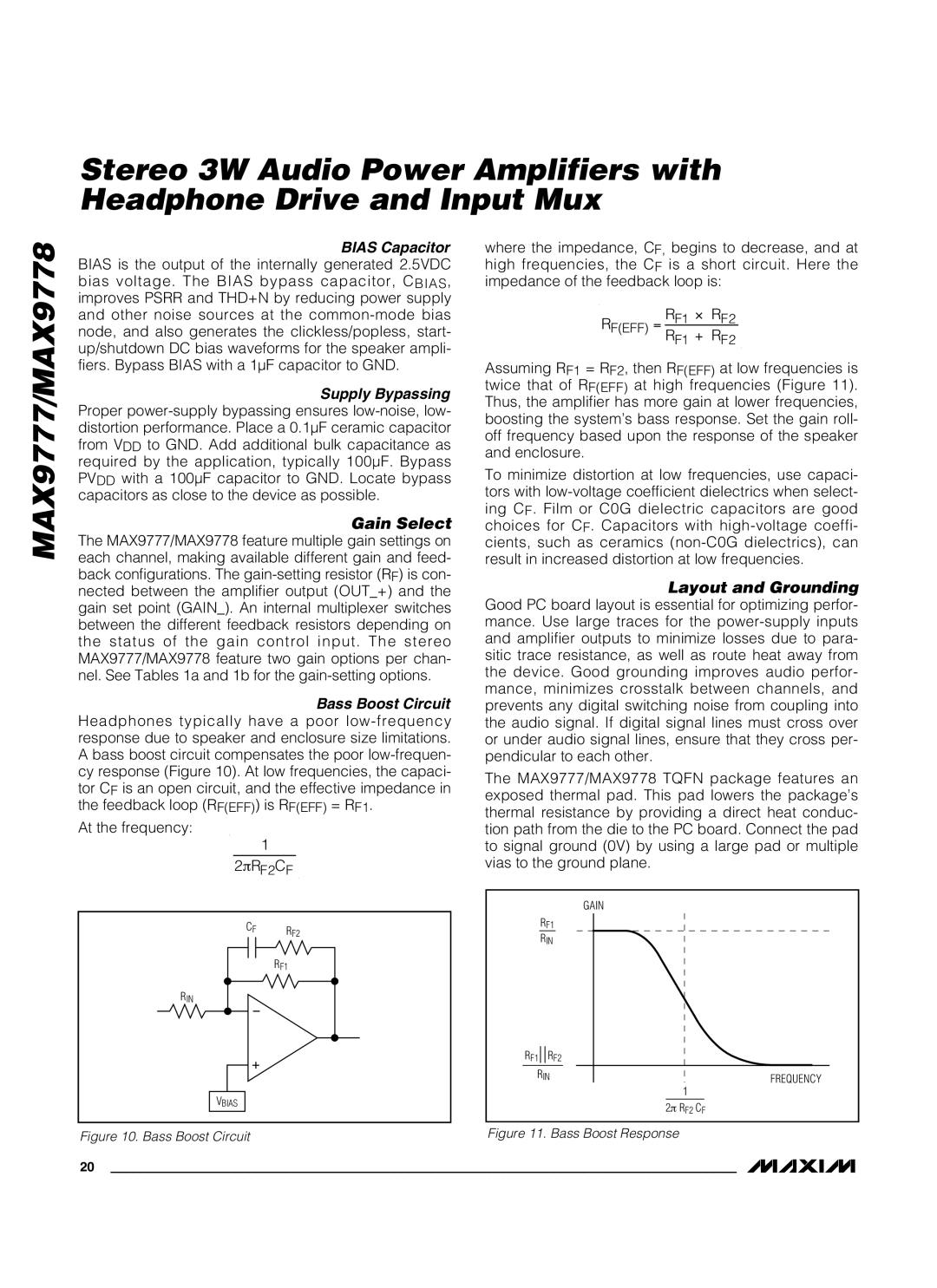
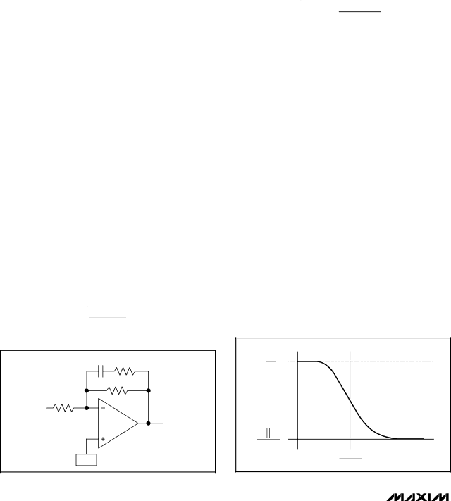
Bass Boost Circuit Headphones typically have a poor low-frequency response due to speaker and enclosure size limitations. A bass boost circuit compensates the poor low-frequen- cy response (Figure 10). At low frequencies, the capaci- tor CF is an open circuit, and the effective impedance in the feedback loop (RF(EFF)) is RF(EFF) = RF1.

At the frequency:

1

2πRF2CF

CF RF2

RF1

RIN

VBIAS

Figure 10. Bass Boost Circuit

where the impedance, CF, begins to decrease, and at high frequencies, the CF is a short circuit. Here the impedance of the feedback loop is:

RF(EFF) = RF1 RF2

RF1 + RF2

Assuming RF1 = RF2, then RF(EFF) at low frequencies is twice that of RF(EFF) at high frequencies (Figure 11). Thus, the amplifier has more gain at lower frequencies, boosting the system’s bass response. Set the gain roll- off frequency based upon the response of the speaker and enclosure.

To minimize distortion at low frequencies, use capaci- tors with low-voltage coefficient dielectrics when select- ing CF. Film or C0G dielectric capacitors are good choices for CF. Capacitors with high-voltage coeffi- cients, such as ceramics (non-C0G dielectrics), can result in increased distortion at low frequencies.

Layout and Grounding

Good PC board layout is essential for optimizing perfor- mance. Use large traces for the power-supply inputs and amplifier outputs to minimize losses due to para- sitic trace resistance, as well as route heat away from the device. Good grounding improves audio perfor- mance, minimizes crosstalk between channels, and prevents any digital switching noise from coupling into the audio signal. If digital signal lines must cross over or under audio signal lines, ensure that they cross per- pendicular to each other.

The MAX9777/MAX9778 TQFN package features an exposed thermal pad. This pad lowers the package’s thermal resistance by providing a direct heat conduc- tion path from the die to the PC board. Connect the pad to signal ground (0V) by using a large pad or multiple vias to the ground plane.


GAIN


RF1


RIN


RF1

RF2


RIN

FREQUENCY


1


2π RF2 CF

Figure 11. Bass Boost Response

20 ______________________________________________________________________________________

Page 20
Image 20
Maxim manual MAX9777/MAX9778, Gain Select, Layout and Grounding, BIAS Capacitor