MAX9777/MAX9778
Stereo 3W Audio Power Amplifiers with Headphone Drive and Input Mux
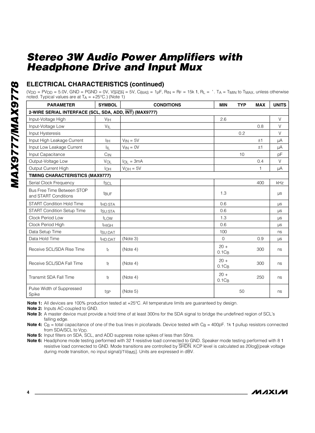
ELECTRICAL CHARACTERISTICS (continued)
(VDD = PVDD = 5.0V, GND = PGND = 0V, VSHDN = 5V, CBIAS = 1µF, RIN = RF = 15kΩ, RL = ∞. TA = TMIN to TMAX, unless otherwise noted. Typical values are at TA = +25°C.) (Note 1)
PARAMETER | SYMBOL | CONDITIONS | MIN | TYP | MAX | UNITS |
|
|
|
|
|
|
|
|
|
|
| |||
VIH |
| 2.6 |
|
| V | |
VIL |
|
|
| 0.8 | V | |
Input Hysteresis |
|
|
| 0.2 |
| V |
|
|
|
|
|
|
|
Input High Leakage Current | IIH | VIN = 5V |
|
| ±1 | µA |
Input Low Leakage Current | IIL | VIN = 0V |
|
| ±1 | µA |
Input Capacitance | CIN |
|
| 10 |
| pF |
VOL | IOL = 3mA |
|
| 0.4 | V | |
Output Current High | IOH | VOH = 5V |
|
| 1 | µA |
TIMING CHARACTERISTICS (MAX9777) |
|
|
|
|
| |
|
|
|
|
|
|
|
Serial Clock Frequency | fSCL |
|
|
| 400 | kHz |
Bus Free Time Between STOP | tBUF |
| 1.3 |
|
| µs |
and START Conditions |
|
|
| |||
|
|
|
|
|
| |
|
|
|
|
|
|
|
START Condition Hold Time | tHD:STA |
| 0.6 |
|
| µs |
START Condition Setup Time | tSU:STA |
| 0.6 |
|
| µs |
Clock Period Low | tLOW |
| 1.3 |
|
| µs |
Clock Period High | tHIGH |
| 0.6 |
|
| µs |
Data Setup Time | tSU:DAT |
| 100 |
|
| ns |
Data Hold Time | tHD:DAT | (Note 3) | 0 |
| 0.9 | µs |
Receive SCL/SDA Rise Time | tr | (Note 4) | 20 + |
| 300 | ns |
0.1CB |
| |||||
|
|
|
|
|
| |
Receive SCL/SDA Fall Time | tf | (Note 4) | 20 + |
| 300 | ns |
0.1CB |
| |||||
|
|
|
|
|
| |
Transmit SDA Fall Time | tf | (Note 4) | 20 + |
| 250 | ns |
0.1CB |
| |||||
|
|
|
|
|
| |
Pulse Width of Suppressed | tSP | (Note 5) |
| 50 |
| ns |
Spike |
|
| ||||
|
|
|
|
|
| |
|
|
|
|
|
|
|
Note 1: All devices are 100% production tested at +25°C. All temperature limits are guaranteed by design.
Note 2: Inputs
Note 3: A master device must provide a hold time of at least 300ns for the SDA signal to bridge the undefined region of SCL’s falling edge.
Note 4: CB = total capacitance of one of the bus lines in picofarads. Device tested with CB = 400pF. 1kΩ pullup resistors connected from SDA/SCL to VDD.
Note 5: Input filters on SDA, SCL, and ADD suppress noise spikes of less than 50ns.
Note 6: Headphone mode testing performed with 32Ω resistive load connected to GND. Speaker mode testing performed with 8Ω resistive load connected to GND. Mode transitions are controlled by SHDN. KCP level is calculated as 20log[(peak voltage during mode transition, no input signal)/1VRMS]. Units are expressed in dBV.
4 _______________________________________________________________________________________