Introducing the |
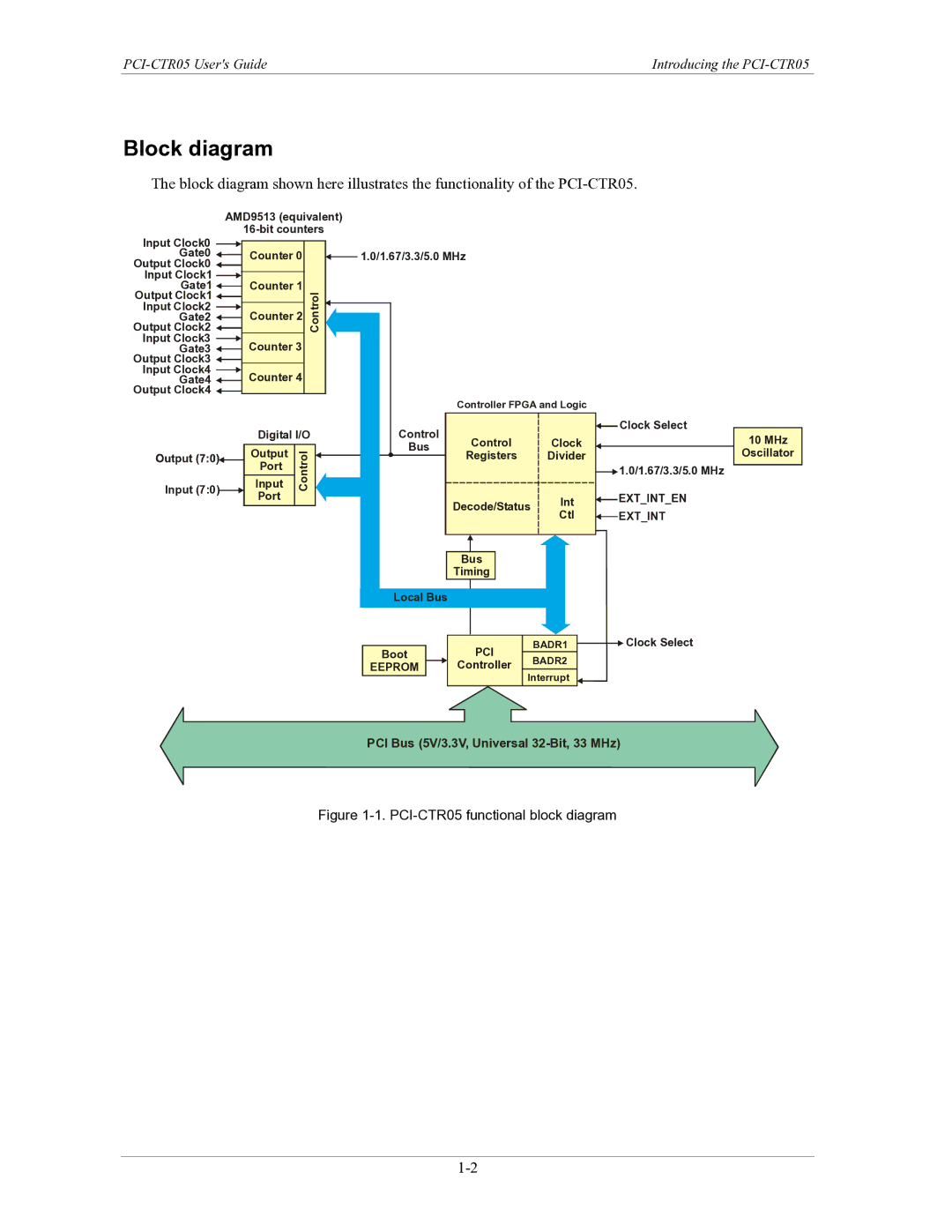
Block diagram
The block diagram shown here illustrates the functionality of the
AMD9513 (equivalent)
Input Clock0
Gate0
Output Clock0
Input Clock1 ![]()
Gate1
Output Clock1
Input Clock2 ![]()
Gate2 ![]()
Output Clock2 ![]()
Input Clock3 ![]()
Gate3 ![]()
Output Clock3
Input Clock4 ![]()
Gate4 ![]()
Output Clock4 ![]()
Counter 0 |
|
|
| 1.0/1.67/3.3/5.0 MHz | ||
|
|
| ||||
Counter 1 | Control |
|
|
|
|
|
Counter 2 |
|
| ||||
| ||||||
|
|
|
|
|
| |
|
|
|
|
|
|
|
Counter 3 |
|
|
|
|
|
|
|
|
|
|
|
|
|
Counter 4 |
|
|
|
|
|
|
|
|
|
|
|
|
|
Controller FPGA and Logic
|
|
|
| Digital I/O |
|
|
|
| Control |
|
|
| Control | ||||
|
|
|
|
|
|
|
|
|
|
| Bus |
|
|
| |||
|
|
|
| Output | Control |
|
|
|
|
|
|
| Registers | ||||
|
|
|
|
|
|
|
|
|
|
|
|
| |||||
|
|
|
| Input |
|
|
|
|
|
|
|
|
|
|
|
| |
Input (7:0) |
|
|
| Port |
|
|
|
|
|
|
|
|
|
|
|
|
|
|
| Port |
|
|
|
|
|
|
|
|
|
|
|
|
| ||
|
|
|
|
|
|
|
| Decode/Status | |||||||||
|
|
|
|
|
|
|
|
| |||||||||
|
|
|
|
|
|
|
|
|
|
|
| ||||||
|
|
|
|
|
|
|
|
|
|
|
|
| |||||
|
|
|
|
|
|
|
|
|
|
|
|
|
|
|
|
|
|
|
|
|
|
|
|
|
|
|
|
|
|
|
|
|
|
|
|
|
|
|
|
|
|
|
|
|
|
|
|
|
| Bus |
| ||
|
|
|
|
|
|
|
|
|
|
|
|
| Timing |
| |||
|
|
|
|
|
|
|
|
|
|
| Local Bus |
|
|
|
|
| |
|
|
|
|
|
|
|
|
|
|
|
|
|
|
|
| ||
![]() Clock Select
Clock Select
Clock
Divider
![]() 1.0/1.67/3.3/5.0 MHz
1.0/1.67/3.3/5.0 MHz
Int ![]() EXT_INT_EN
EXT_INT_EN
Ctl ![]() EXT_INT
EXT_INT
10MHz Oscillator
|
|
| PCI | BADR1 |
|
| Clock Select |
Boot |
|
|
|
| |||
|
| BADR2 |
|
|
| ||
EEPROM |
|
| Controller |
|
|
| |
|
|
|
|
| |||
|
| Interrupt |
|
|
| ||
|
|
|
|
|
|
|
PCI Bus (5V/3.3V, Universal