Electrical and Logical Differences
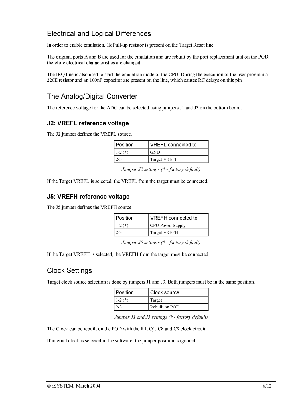
In order to enable emulation, 1k
The original ports A and B are used for the emulation and are rebuilt by the port replacement unit on the POD; therefore electrical characteristics are changed.
The IRQ line is also used to start the emulation mode of the CPU. During the execution of the user program a 220E resistor and an 100nF capacitor are present on the line, which causes RC delays on this pin.
The Analog/Digital Converter
The reference voltage for the ADC can be selected using jumpers J1 and J3 on the bottom board.
J2: VREFL reference voltage
The J2 jumper defines the VREFL source.
Position | VREFL connected to |
GND | |
Target VREFL |
Jumper J2 settings (* - factory default)
If the Target VREFL is selected, the VREFL from the target must be connected.
J5: VREFH reference voltage
The J5 jumper defines the VREFH source.
Position | VREFH connected to |
CPU Power Supply | |
Target VREFH |
Jumper J5 settings (* - factory default)
If the Target VREFH is selected, the VREFH from the target must be connected.
Clock Settings
Target clock source selection is done by jumpers J1 and J3. Both jumpers must be in the same position.
Position | Clock source |
Target | |
Rebuilt on POD |
Jumper J1 and J3 settings (* - factory default)
The Clock can be rebuilt on the POD with the R1, Q1, C8 and C9 clock circuit.
If internal clock is selected in the software, the jumper position is ignored.
iSYSTEM, March 2004 | 6/12 |
