C M L 1 2 S D P 2 5 6 | 0 7 / 1 7 / 0 2 |
JP1 will isolate the SCI0 RXD pin from the transceiver.
The 1,4,6,7,8, and 9 pins provide RS232 flow control and status. These are connected on the on the bottom of the development board to provide NULL status to the host. User may isolate pins and provide flow control or status connection to the host by applying HCS12 I/O signals and RS232 level conversion.
P_COM2
P_COM2 is a 3 pin header that provides the HCS12 SCI1 serial port translated to RS232 signal levels. A solder cup DB9 style connector may be installed with wires and connector to apply this channel. JP2 option will isolate the SCI RXD pin from the transceiver.
P_COM2 pin connections:
Pin 1 = TXD
Pin 2 = RXD
Pin 3 = GND / common
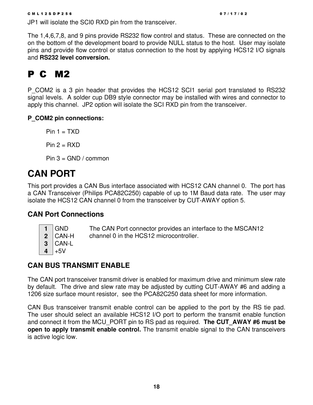
CAN PORT
This port provides a CAN Bus interface associated with HCS12 CAN channel 0. The port has a CAN Transceiver (Philips PCA82C250) capable of up to 1M Baud data rate. The user may isolate the HCS12 CAN channel 0 from the transceiver by
CAN Port Connections
1
2
3
4
GND | The CAN Port connector provides an interface to the MSCAN12 |
| channel 0 in the HCS12 microcontroller. |
|
|
+5V |
|
CAN BUS TRANSMIT ENABLE
The CAN port transceiver transmit driver is enabled for maximum drive and minimum slew rate by default. The drive and slew rate may be adjusted by cutting
CAN Bus transceiver transmit enable control can be applied to the port by the RS tie pad. The user should select an available HCS12 I/O port to perform the transmit enable function and connect it from the MCU_PORT pin to RS pad as required. The CUT_AWAY #6 must be open to apply transmit enable control. The transmit enable signal to the CAN transceivers is active logic low.
18