C M L 1 2 S D P 2 5 6 | 0 7 / 1 7 / 0 2 |
NOTES:
1)The LCD write requires 3 SPI transfers. Transfer 1 provides data 0 - 3 and RS (register select) value. Transfer 2 provides the same data with the EN (D7) bit set. Transfer 3 provides same data with the EN bit clear.
2)Resistor R25 can be removed to apply and external VEE potential.
3)
BDM PORT
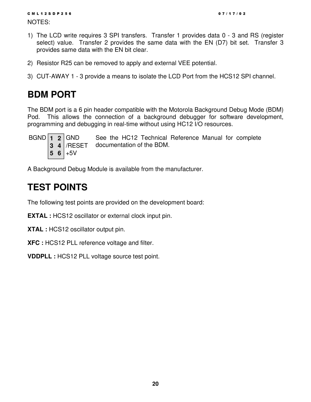
The BDM port is a 6 pin header compatible with the Motorola Background Debug Mode (BDM) Pod. This allows the connection of a background debugger for software development, programming and debugging in
BGND
1 | 2 | GND | See the HC12 Technical Reference Manual for complete |
3 | 4 | /RESET | documentation of the BDM. |
5 | 6 | +5V |
|
|
|
|
|
A Background Debug Module is available from the manufacturer.
TEST POINTS
The following test points are provided on the development board:
EXTAL : HCS12 oscillator or external clock input pin.
XTAL : HCS12 oscillator output pin.
XFC : HCS12 PLL reference voltage and filter.
VDDPLL : HCS12 PLL voltage source test point.
20