Technical Description
Port C
Port C is written and read to as a single eight bit port, but it has the ability to be configured as two four bit ports. If both lower and upper nibbles are configure the same then no special considerations need to be made. But if they are configured differently, one nibble as input, and one as output then the user will have to keep this in mind. When reading, the input will be returned on the corresponding upper or lower nibble while the current outputs will be returned on their corresponding upper or lower nibble. When writing, the corresponding nibble will be written to the output nibble, while the input nibble will have its output register written to. The output register can be written to without affecting the inputs.
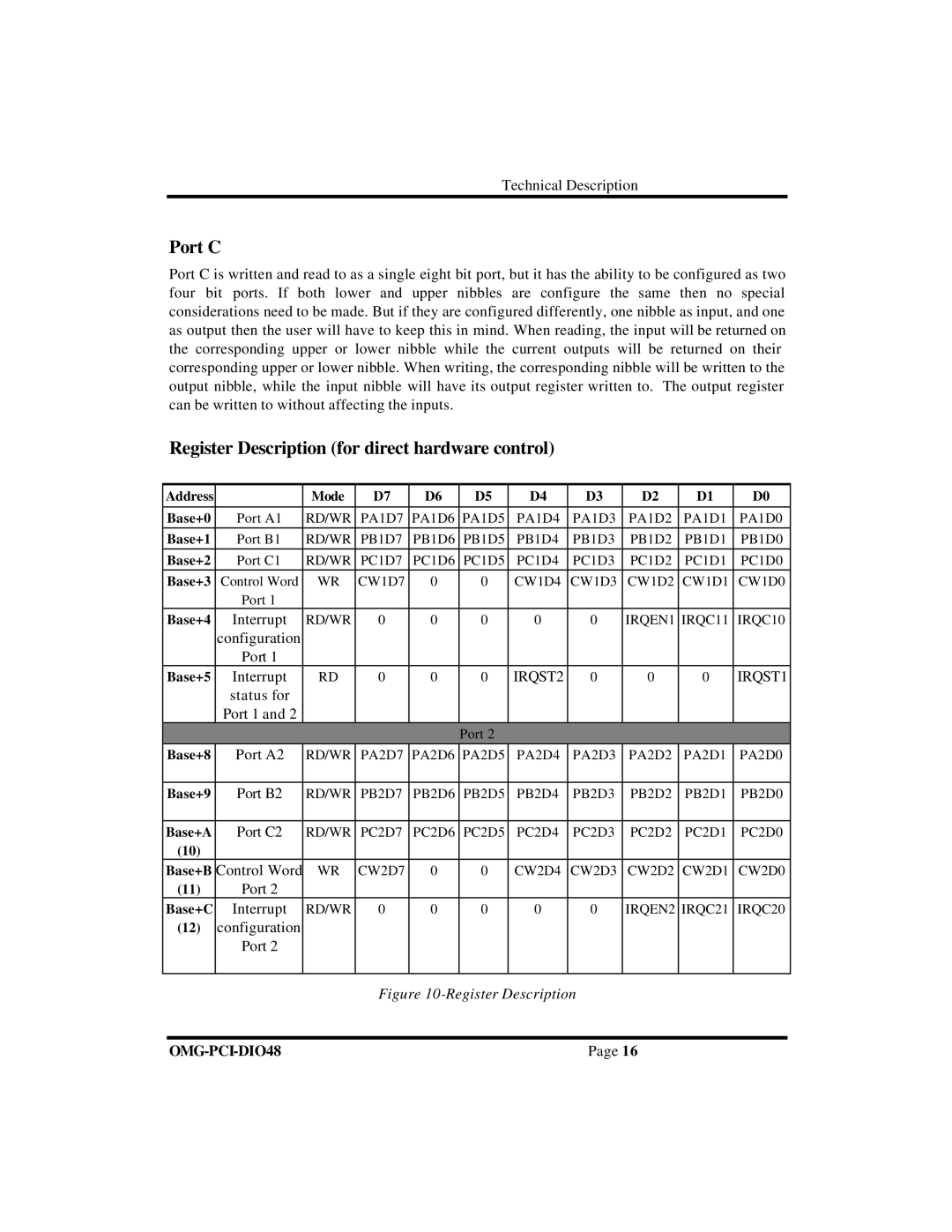
Register Description (for direct hardware control)
Address |
| Mode | D7 | D6 | D5 | D4 | D3 | D2 | D1 | D0 |
|
|
|
|
|
|
|
|
|
|
|
Base+0 | Port A1 | RD/WR | PA1D7 | PA1D6 | PA1D5 | PA1D4 | PA1D3 | PA1D2 | PA1D1 | PA1D0 |
Base+1 | Port B1 | RD/WR | PB1D7 | PB1D6 | PB1D5 | PB1D4 | PB1D3 | PB1D2 | PB1D1 | PB1D0 |
Base+2 | Port C1 | RD/WR | PC1D7 | PC1D6 | PC1D5 | PC1D4 | PC1D3 | PC1D2 | PC1D1 | PC1D0 |
Base+3 | Control Word | WR | CW1D7 | 0 | 0 | CW1D4 | CW1D3 | CW1D2 | CW1D1 | CW1D0 |
| Port 1 |
|
|
|
|
|
|
|
|
|
Base+4 | Interrupt | RD/WR | 0 | 0 | 0 | 0 | 0 | IRQEN1 | IRQC11 | IRQC10 |
| configuration |
|
|
|
|
|
|
|
|
|
| Port 1 |
|
|
|
|
|
|
|
|
|
Base+5 | Interrupt | RD | 0 | 0 | 0 | IRQST2 | 0 | 0 | 0 | IRQST1 |
| status for |
|
|
|
|
|
|
|
|
|
| Port 1 and 2 |
|
|
|
|
|
|
|
|
|
|
|
|
|
| Port 2 |
|
|
|
|
|
Base+8 | Port A2 | RD/WR | PA2D7 | PA2D6 | PA2D5 | PA2D4 | PA2D3 | PA2D2 | PA2D1 | PA2D0 |
|
|
|
|
|
|
|
|
|
|
|
Base+9 | Port B2 | RD/WR | PB2D7 | PB2D6 | PB2D5 | PB2D4 | PB2D3 | PB2D2 | PB2D1 | PB2D0 |
|
|
|
|
|
|
|
|
|
|
|
Base+A | Port C2 | RD/WR | PC2D7 | PC2D6 | PC2D5 | PC2D4 | PC2D3 | PC2D2 | PC2D1 | PC2D0 |
(10) |
|
|
|
|
|
|
|
|
|
|
Base+B | Control Word | WR | CW2D7 | 0 | 0 | CW2D4 | CW2D3 | CW2D2 | CW2D1 | CW2D0 |
(11) | Port 2 |
|
|
|
|
|
|
|
|
|
Base+C | Interrupt | RD/WR | 0 | 0 | 0 | 0 | 0 | IRQEN2 | IRQC21 | IRQC20 |
(12) | configuration |
|
|
|
|
|
|
|
|
|
| Port 2 |
|
|
|
|
|
|
|
|
|
|
|
|
|
|
|
|
|
|
|
|
Figure 10-Register Description
| Page 16 |