14.Wiring Connection Diagram
15.Terminal Function of IC's
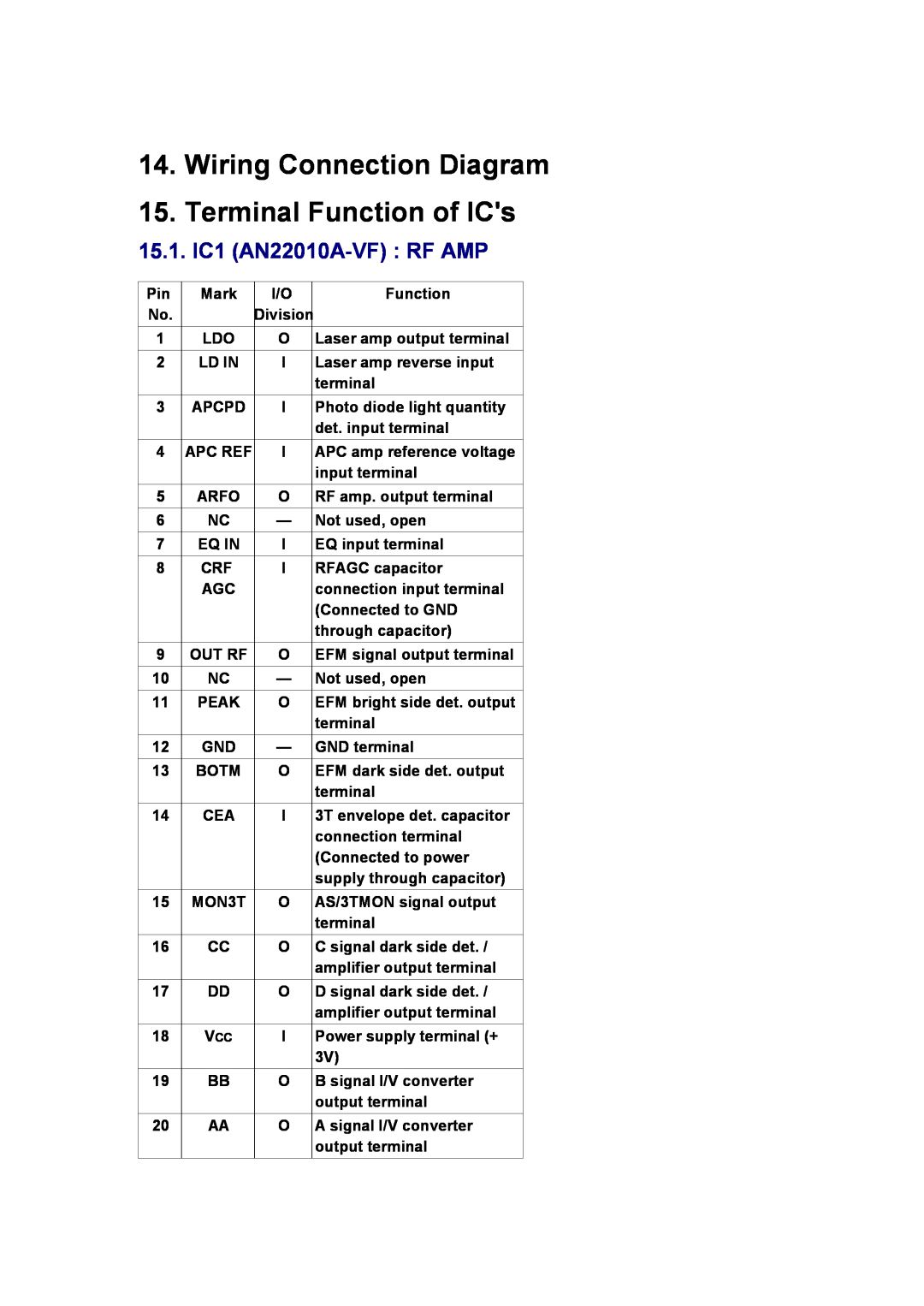
15.1. IC1 (AN22010A-VF) : RF AMP
Pin | Mark | I/O | Function |
No. |
| Division |
|
1 | LDO | O | Laser amp output terminal |
2 | LD IN | I | Laser amp reverse input |
|
|
| terminal |
3 | APCPD | I | Photo diode light quantity |
|
|
| det. input terminal |
4 | APC REF | I | APC amp reference voltage |
|
|
| input terminal |
5 | ARFO | O | RF amp. output terminal |
6 | NC | — | Not used, open |
7 | EQ IN | I | EQ input terminal |
8 | CRF | I | RFAGC capacitor |
| AGC |
| connection input terminal |
|
|
| (Connected to GND |
|
|
| through capacitor) |
9 | OUT RF | O | EFM signal output terminal |
10 | NC | — | Not used, open |
11 | PEAK | O | EFM bright side det. output |
|
|
| terminal |
12 | GND | — | GND terminal |
13 | BOTM | O | EFM dark side det. output |
|
|
| terminal |
14 | CEA | I | 3T envelope det. capacitor |
|
|
| connection terminal |
|
|
| (Connected to power |
|
|
| supply through capacitor) |
15 | MON3T | O | AS/3TMON signal output |
|
|
| terminal |
16 | CC | O | C signal dark side det. / |
|
|
| amplifier output terminal |
17 | DD | O | D signal dark side det. / |
|
|
| amplifier output terminal |
18 | VCC | I | Power supply terminal (+ |
|
|
| 3V) |
19 | BB | O | B signal I/V converter |
|
|
| output terminal |
20 | AA | O | A signal I/V converter |
|
|
| output terminal |