Interfacing
This dual scan
Planar Application Note 116 summarizes some of the interfacing options that have been used in the past with EL VGA displays.
Video Input Signals
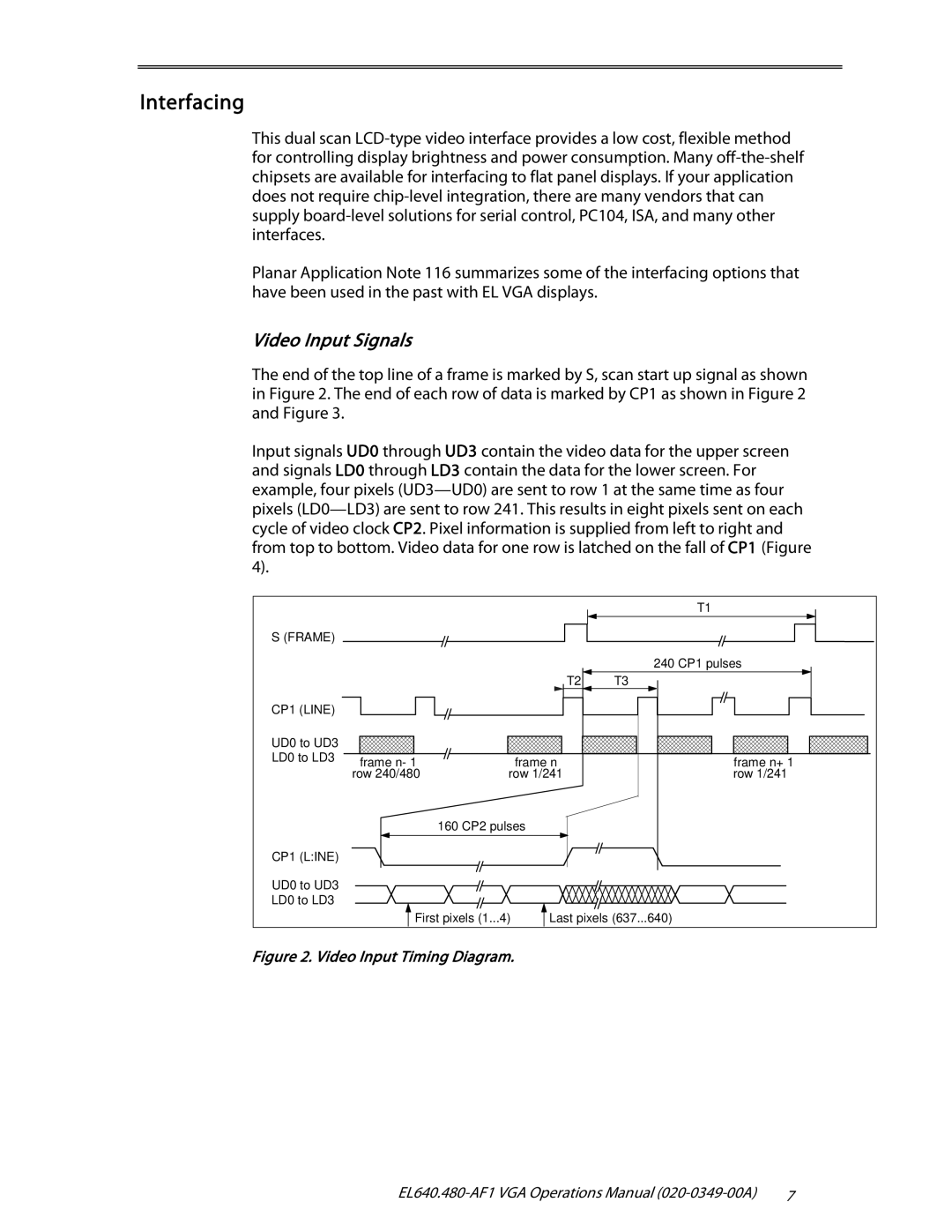
The end of the top line of a frame is marked by S, scan start up signal as shown in Figure 2. The end of each row of data is marked by CP1 as shown in Figure 2 and Figure 3.
Input signals UD0 through UD3 contain the video data for the upper screen and signals LD0 through LD3 contain the data for the lower screen. For example, four pixels
|
|
|
| T1 |
S (FRAME) |
|
|
|
|
|
|
|
| 240 CP1 pulses |
|
|
| T2 | T3 |
CP1 (LINE) |
|
|
|
|
UD0 to UD3 |
|
|
|
|
LD0 to LD3 | frame n- 1 | frame n | frame n+ 1 | |
| row 240/480 | row 1/241 | row 1/241 | |
|
| 160 CP2 pulses |
|
|
CP1 (L:INE) |
|
|
|
|
UD0 to UD3 |
|
|
|
|
LD0 to LD3 |
|
|
|
|
| First pixels (1...4) | Last pixels (637...640) | ||
Figure 2. Video Input Timing Diagram.
7 |