
EL320.256-FD7, High Brightness, High Contrast Display specifications
The Planar EL320.256-FD7 is a cutting-edge display solution renowned for its high contrast and high brightness attributes, making it an ideal choice for various demanding applications. With a focus on delivering superior visual performance, this display has gained popularity in both commercial and industrial sectors.One of the standout features of the Planar EL320.256-FD7 is its impressive high brightness capability. This display can produce bright images even in high ambient light environments, which is essential for applications such as outdoor signage, public information displays, and command and control centers. The display's brightness ensures that content remains visible and accessible, regardless of surrounding lighting conditions.
In addition to its brightness, the EL320.256-FD7 boasts a remarkable contrast ratio. This feature enhances image clarity and allows for deeper blacks and more vivid colors. The high contrast not only improves the overall quality of the display but also reduces eye strain, making it suitable for long viewing periods in various settings. Whether in an office environment or a high-stakes control room, the display's characteristics ensure effective communication of information.
The technology behind the Planar EL320.256-FD7 incorporates advanced display technologies that contribute to its robust performance. The use of high-quality LCD panels and precision engineering helps achieve a consistent and reliable visual output. Furthermore, it supports a wide range of color depths, providing lifelike images and enabling the display to engage audiences effectively.
Reliability is another critical characteristic of the EL320.256-FD7. The display is built to endure extended usage and operates efficiently in various environmental conditions. This durability makes it suitable for mission-critical applications where downtime is not an option.
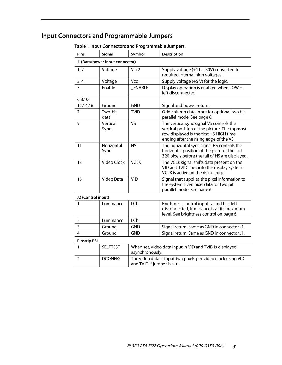
Connectivity options on the Planar EL320.256-FD7 are also impressive. It is equipped with multiple input interfaces, allowing seamless integration with various devices and systems. This flexibility ensures that users can easily connect the display to computers, media players, and other peripherals without hassle.
In conclusion, the Planar EL320.256-FD7 is a robust high contrast, high brightness display that excels in numerous applications. With its excellent image quality, durability, and versatile connectivity options, it represents an ideal solution for any organization looking to enhance their visual communication capabilities. Whether for advertising, information dissemination, or control systems, the EL320.256-FD7 stands out as a premium choice in the display market.