Manuals
/
RAD Data comm
/
Computer Equipment
/
Network Router
RAD Data comm
100 DB-25 Pin Allocation V.35, V.11, used for RS-530, X.21, Name, Type
Models:
100
1
9
9
Download
9 pages
25.47 Kb
2
3
4
5
6
7
8
9
Page 9
Image 9
Page 8
Page 9
Page 9
Image 9
Page 8
Page 9
Contents
TinyBridge-100
ORDERING
Miniature Remote Fast
Ethernet Bridge
Wire-speed WAN throughput 19,700 pps at 10 Mbps 10/100BaseT interface
FEATURES
Fault propagation of WAN error conditions to LAN port
DESCRIPTION
APPLICATIONS
Figure 2. Receive and Transmit Clock Timing Diagrams
5ns 5ns
FLAG
Figure 5. Extending Ethernet over 4-Wires in the Campus Enviroment
SPECIFICATIONS
ETHERNET
Figure 6. Broadcasting Data over Satellite Link
4-wire Range
SAFETY
Connectors
Power Supply
ACHTUNG
Sicherheitshinweise
DECLARATION OF CONFORMITY
declares that the product
Configuring TinyBridge-100
INSTALLATION
Table 1. DIP Switch Settings
Connecting the LAN Interface
Figure 7. Connecting the 4-wire WAN Interface Connecting Power
Table 2. LED Indicators
OPERATION
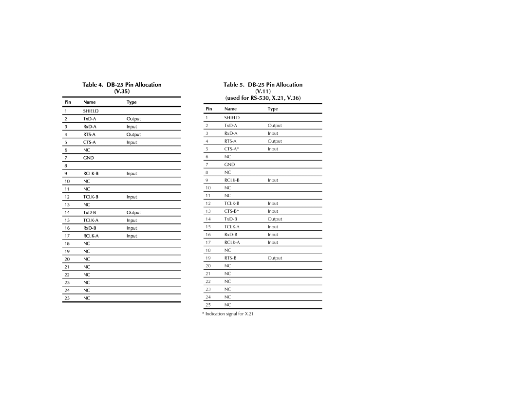
Table 3. DB-25 Pin Allocation
Table 5. DB-25 Pin Allocation
Table 4. DB-25 Pin Allocation V.35
V.11
used for RS-530, X.21
Top
Page
Image
Contents