Chapter 3.

Introduction

Theory of Operation

Potential Wells

Advanced CCD Theory

The charge-coupled device (CCD) is the imager of choice for use in quantitative image acquisition systems. This chapter familiarizes you with CCDs and the terminology used in describing them. It also discusses CCD performance characteristics. If these are already familiar topics, you may still find this chapter useful as a refresher or a reference.

Most CCD imagers are made from silicon, because of its properties when exposed to electromagnetic radiation in the visible spectrum.

In crystalline silicon, each atom is covalently bonded to its neighbors. Incident photons that penetrate the lattice can break these bonds and generate electron- hole pairs. Silicon becomes transparent at 1000–1100 nm and is opaque to light at wavelengths shorter than 400 nm. The photon-produced electronic charge is proportional to the incident light between these wavelength limits.

However, charge can be created by other energy sources. High-energy particles, x-rays, and cosmic rays can break many thousands of bonds. Excessive exposure can damage the crystal lattice.

Bonds can also be broken by thermal agitation. The rate of electron-hole pair generation due to thermal energy is dependent on temperature and can be reduced arbitrarily through cooling. The unwanted charge produced by thermal agitation is called dark current, because it is produced in the absence of light.

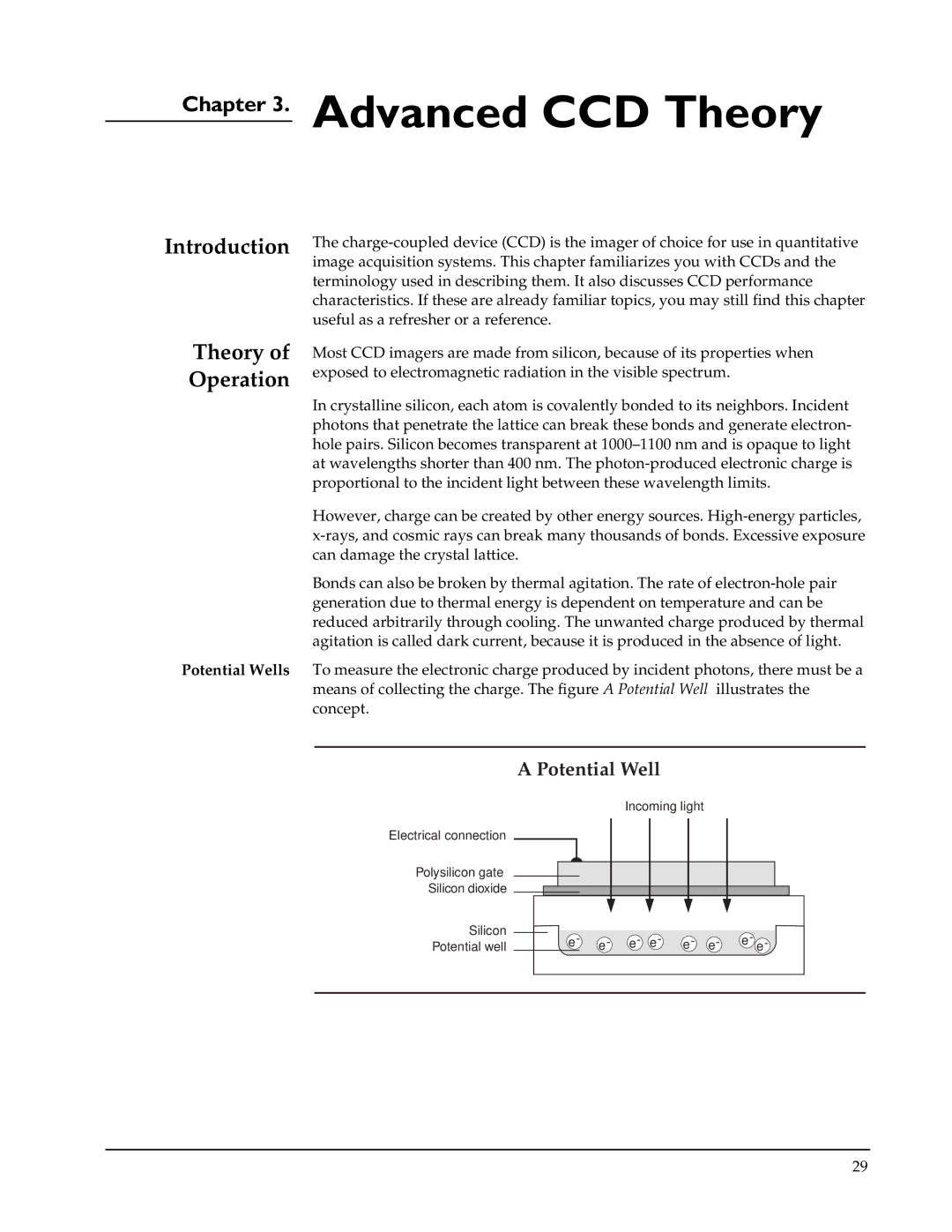
To measure the electronic charge produced by incident photons, there must be a means of collecting the charge. The figure A Potential Well illustrates the concept.

A Potential Well

Electrical connection

Polysilicon gate Silicon dioxide

Silicon

Potential well

Incoming light

e-

e-

e- e-

e-

e-

e- e-

29

Page 35
Image 35
Roper Photometric manual Introduction Theory of Operation, Potential Wells