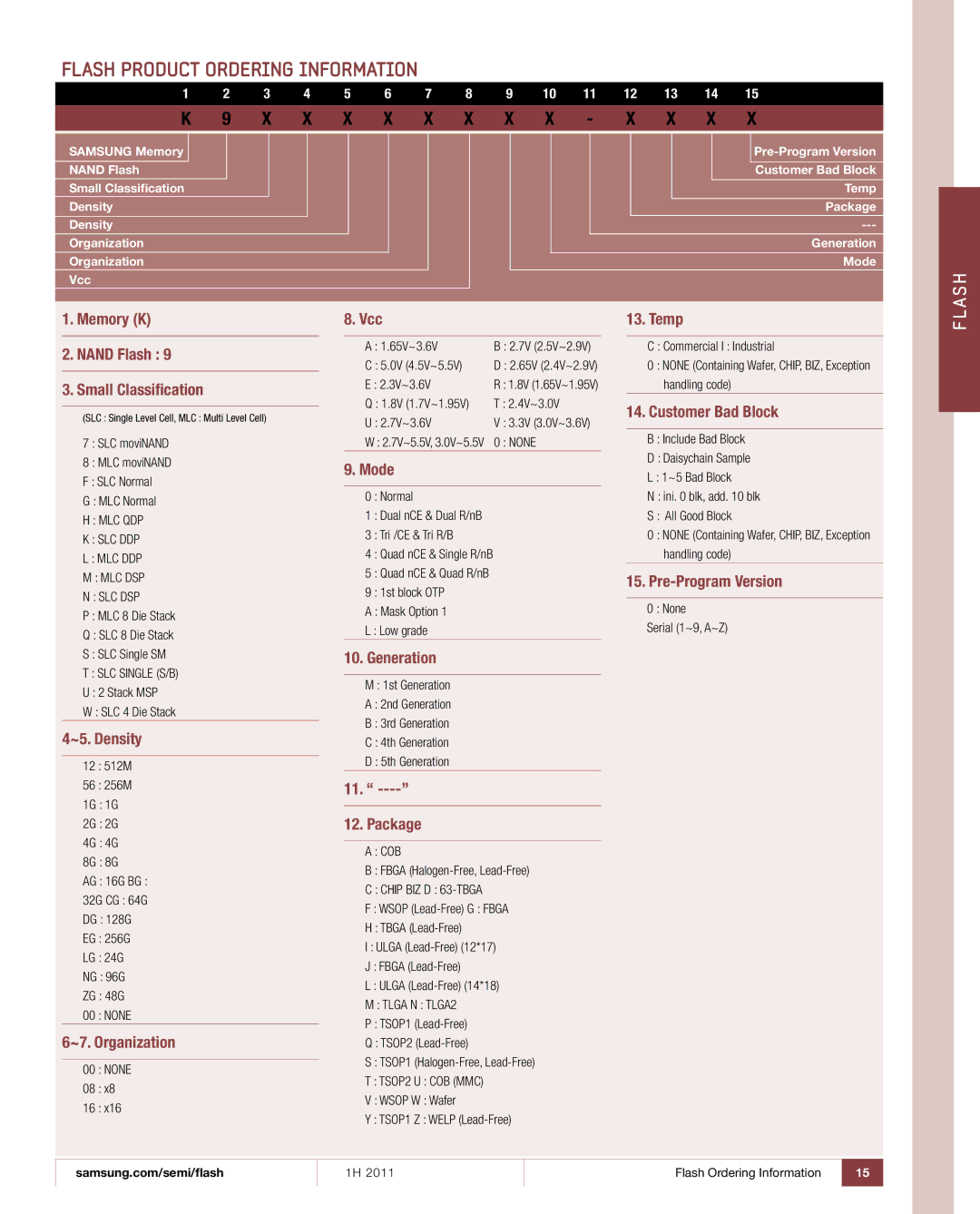
FLASH Product Ordering Information
1 | 2 | 3 | 4 | 5 | 6 | 7 | 8 | 9 | 10 | 11 | 12 | 13 | 14 | 15 |
K | 9 | X | X | X | X | X | X | X | X | - | X | X | X | X |
|
|
|
|
|
|
|
|
|
|
|
|
|
|
|
SAMSUNG Memory |
|
|
|
|
|
|
|
|
|
|
|
|
| |
NAND Flash |
|
|
|
|
|
|
|
|
|
|
|
|
| Customer Bad Block |
Small Classification |
|
|
|
|
|
|
|
|
|
|
|
|
| Temp |
Density |
|
|
|
|
|
|
|
|
|
|
|
|
| Package |
Density |
|
|
|
|
|
|
|
|
|
|
|
|
| |
Organization |
|
|
|
|
|
|
|
|
|
|
|
|
| Generation |
Organization |
|
|
|
|
|
|
|
|
|
|
|
|
| Mode |
Vcc |
|
|
|
|
|
|
|
|
|
|
|
|
|
|
|
|
|
|
|
|
|
|
|
|
|
|
|
|
|
A SH
1.Memory (K)
2.NAND Flash : 9
3.Small Classification
(SLC : Single Level Cell, MLC : Multi Level Cell)
7 : SLC moviNAND
8 : MLC moviNAND
F : SLC Normal
G : MLC Normal
H : MLC QDP
K : SLC DDP
L : MLC DDP
M : MLC DSP
N : SLC DSP
P : MLC 8 Die Stack
Q : SLC 8 Die Stack
S : SLC Single SM
T : SLC SINGLE (S/B)
U : 2 Stack MSP
W : SLC 4 Die Stack
4~5. Density
12 : 512M
56 : 256M
1G : 1G
2G : 2G
4G : 4G
8G : 8G
AG : 16G BG :
32G CG : 64G
DG : 128G
EG : 256G
LG : 24G
NG : 96G
ZG : 48G
00 : NONE
6~7. Organization
00 : NONE
08 : x8
16 : x16
8. Vcc
A : 1.65V~3.6V | B : 2.7V (2.5V~2.9V) |
C : 5.0V (4.5V~5.5V) | D : 2.65V (2.4V~2.9V) |
E : 2.3V~3.6V | R : 1.8V (1.65V~1.95V) |
Q : 1.8V (1.7V~1.95V) | T : 2.4V~3.0V |
U : 2.7V~3.6V | V : 3.3V (3.0V~3.6V) |
W : 2.7V~5.5V, 3.0V~5.5V | 0 : NONE |
9. Mode |
|
0 : Normal
1 : Dual nCE & Dual R/nB
3 : Tri /CE & Tri R/B
4 : Quad nCE & Single R/nB
5 : Quad nCE & Quad R/nB
9 : 1st block OTP
A : Mask Option 1
L : Low grade
10. Generation
M : 1st Generation
A : 2nd Generation
B : 3rd Generation
C : 4th Generation
D : 5th Generation
11.“
12.Package
A : COB
B : FBGA
C : CHIP BIZ D : 63-TBGA
F : WSOP
H : TBGA
I : ULGA
J : FBGA
L : ULGA
M : TLGA N : TLGA2
P : TSOP1
Q : TSOP2
S : TSOP1
T : TSOP2 U : COB (MMC)
V : WSOP W : Wafer
Y : TSOP1 Z : WELP
13. Temp
C : Commercial I : Industrial
0 : NONE (Containing Wafer, CHIP, BIZ, Exception
handling code)
14. Customer Bad Block
B : Include Bad Block
D : Daisychain Sample
L : 1~5 Bad Block
N : ini. 0 blk, add. 10 blk
S : All Good Block
0 : NONE (Containing Wafer, CHIP, BIZ, Exception handling code)
15.
0 : None
Serial (1~9, A~Z)
FL
samsung.com/semi/flash
1H 2011
Flash Ordering Information | 15 |
|
|