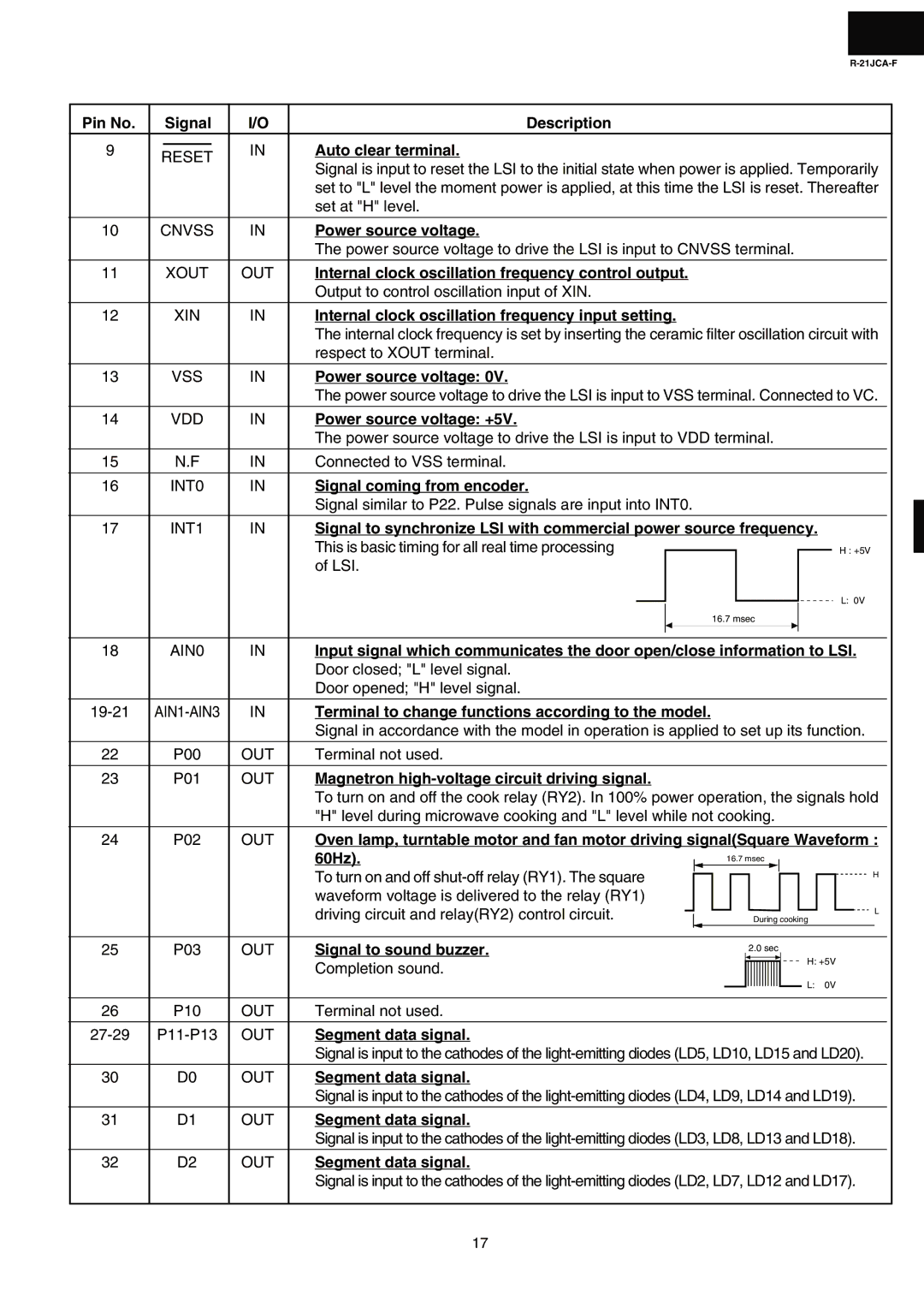
Pin No. |
| Signal | I/O | Description |
|
|
|
|
|
|
|
|
|
|
|
|
|
|
|
|
|
| ||||||
9 |
|
|
| IN | Auto clear terminal. |
|
|
|
|
|
|
|
|
|
|
|
|
|
|
|
|
|
| |||||
RESET |
|
|
|
|
|
|
|
|
|
|
|
|
|
|
|
|
|
| ||||||||||
|
| Signal is input to reset the LSI to the initial state when power is applied. Temporarily |
| |||||||||||||||||||||||||
|
|
|
|
|
| |||||||||||||||||||||||
|
|
|
|
| set to "L" level the moment power is applied, at this time the LSI is reset. Thereafter |
| ||||||||||||||||||||||
|
|
|
|
| set at "H" level. |
|
|
|
|
|
|
|
|
|
|
|
|
|
|
|
|
|
| |||||
|
|
|
|
|
|
|
|
|
|
|
|
|
|
|
|
|
|
|
|
|
|
|
|
|
|
|
|
|
10 | CNVSS | IN | Power source voltage. |
|
|
|
|
|
|
|
|
|
|
|
|
|
|
|
|
|
| |||||||
|
|
|
|
| The power source voltage to drive the LSI is input to CNVSS terminal. |
| ||||||||||||||||||||||
|
|
|
|
|
|
|
|
|
|
|
|
|
|
|
|
|
|
|
|
|
|
|
|
|
|
|
|
|
11 |
| XOUT | OUT | Internal clock oscillation frequency control output. |
|
|
|
|
|
|
|
|
|
|
|
|
|
|
|
|
|
| ||||||
|
|
|
|
| Output to control oscillation input of XIN. |
|
|
|
|
|
|
|
|
|
|
|
|
|
|
|
|
|
| |||||
|
|
|
|
|
|
|
|
|
|
|
|
|
|
|
|
|
|
|
|
|
|
|
|
|
|
|
|
|
12 |
| XIN | IN | Internal clock oscillation frequency input setting. |
|
|
|
|
|
|
|
|
|
|
|
|
|
|
|
|
|
| ||||||
|
|
|
|
| The internal clock frequency is set by inserting the ceramic filter oscillation circuit with |
| ||||||||||||||||||||||
|
|
|
|
| respect to XOUT terminal. |
|
|
|
|
|
|
|
|
|
|
|
|
|
|
|
|
|
| |||||
13 |
| VSS | IN | Power source voltage: 0V. |
|
|
|
|
|
|
|
|
|
|
|
|
|
|
|
|
|
| ||||||
|
|
|
|
| The power source voltage to drive the LSI is input to VSS terminal. Connected to VC. |
| ||||||||||||||||||||||
|
|
|
|
|
|
|
|
|
|
|
|
|
|
|
|
|
|
|
|
|
|
|
|
|
|
|
|
|
14 |
| VDD | IN | Power source voltage: +5V. |
|
|
|
|
|
|
|
|
|
|
|
|
|
|
|
|
|
| ||||||
|
|
|
|
| The power source voltage to drive the LSI is input to VDD terminal. |
| ||||||||||||||||||||||
15 |
| N.F | IN | Connected to VSS terminal. |
|
|
|
|
|
|
|
|
|
|
|
|
|
|
|
|
|
| ||||||
|
|
|
|
|
|
|
|
|
|
|
|
|
|
|
|
|
|
|
|
|
|
|
|
|
|
|
|
|
16 |
| INT0 | IN | Signal coming from encoder. |
|
|
|
|
|
|
|
|
|
|
|
|
|
|
|
|
|
| ||||||
|
|
|
|
| Signal similar to P22. Pulse signals are input into INT0. |
|
|
|
|
|
|
|
|
|
|
|
|
|
|
|
|
|
| |||||
17 |
| INT1 | IN | Signal to synchronize LSI with commercial power source frequency. |
| |||||||||||||||||||||||
|
|
|
|
| This is basic timing for all real time processing |
|
|
|
|
|
|
|
|
|
|
|
|
|
|
|
|
|
|
| H : +5V |
| ||
|
|
|
|
| of LSI. |
|
|
|
|
|
|
|
|
|
|
|
|
|
|
|
|
|
|
|
|
|
| |
|
|
|
|
|
|
|
|
|
|
|
|
|
|
|
|
|
|
|
|
|
|
|
|
|
| L: 0V |
| |
|
|
|
|
|
|
|
|
|
|
| 16.7 msec |
|
| |||||||||||||||
|
|
|
|
|
|
|
|
|
|
|
|
|
|
|
| |||||||||||||
|
|
|
|
|
|
|
|
|
|
|
|
|
|
|
|
|
|
|
|
|
|
|
|
|
|
|
| |
|
|
|
|
|
|
|
|
|
|
|
|
|
|
|
|
|
|
|
|
|
|
|
|
|
|
|
|
|
18 |
| AIN0 | IN | Input signal which communicates the door open/close information to LSI. |
| |||||||||||||||||||||||
|
|
|
|
| Door closed; "L" level signal. |
|
|
|
|
|
|
|
|
|
|
|
|
|
|
|
|
|
| |||||
|
|
|
|
| Door opened; "H" level signal. |
|
|
|
|
|
|
|
|
|
|
|
|
|
|
|
|
|
| |||||
|
|
|
|
|
|
|
|
|
|
|
|
|
|
|
|
|
|
|
|
|
|
|
|
|
|
|
|
|
IN | Terminal to change functions according to the model. |
|
|
|
|
|
|
|
|
|
|
|
|
|
|
|
|
|
| |||||||||
|
|
|
|
| Signal in accordance with the model in operation is applied to set up its function. |
| ||||||||||||||||||||||
|
|
|
|
|
|
|
|
|
|
|
|
|
|
|
|
|
|
|
|
|
|
|
|
|
|
|
|
|
22 |
| P00 | OUT | Terminal not used. |
|
|
|
|
|
|
|
|
|
|
|
|
|
|
|
|
|
| ||||||
|
|
|
|
|
|
|
|
|
|
|
|
|
|
|
|
|
|
|
|
|
|
|
|
|
|
|
|
|
23 |
| P01 | OUT | Magnetron |
|
|
|
|
|
|
|
|
|
|
|
|
|
|
|
|
|
| ||||||
|
|
|
|
| To turn on and off the cook relay (RY2). In 100% power operation, the signals hold |
| ||||||||||||||||||||||
|
|
|
|
| "H" level during microwave cooking and "L" level while not cooking. |
| ||||||||||||||||||||||
|
|
|
|
|
|
|
|
|
|
|
|
|
|
|
|
|
|
|
|
|
|
|
|
|
|
|
| |
24 |
| P02 | OUT | Oven lamp, turntable motor and fan motor driving signal(Square Waveform : |
| |||||||||||||||||||||||
|
|
|
|
| 60Hz). |
|
|
| 16.7 msec |
|
|
|
|
|
| |||||||||||||
|
|
|
|
|
|
|
| |||||||||||||||||||||
|
|
|
|
|
|
|
|
|
|
|
|
|
|
|
|
|
|
|
|
|
|
|
|
|
| H |
| |
|
|
|
|
| To turn on and off |
|
|
|
|
|
|
|
|
|
|
|
|
|
|
|
| |||||||
|
|
|
|
|
|
|
|
|
|
|
|
|
|
|
|
|
|
|
|
|
|
| ||||||
|
|
|
|
| waveform voltage is delivered to the relay (RY1) |
|
|
|
|
|
|
|
|
|
|
|
|
|
|
|
|
|
| |||||
|
|
|
|
| driving circuit and relay(RY2) control circuit. |
|
|
|
|
|
|
|
|
|
|
|
|
|
|
|
|
|
| L |
| |||
|
|
|
|
|
|
|
|
|
|
| During cooking |
| ||||||||||||||||
|
|
|
|
|
|
|
|
|
|
|
|
|
|
|
|
|
|
|
|
|
|
|
|
|
|
|
|
|
25 |
| P03 | OUT | Signal to sound buzzer. |
|
|
| 2.0 sec |
|
| ||||||||||||||||||
|
|
|
|
| Completion sound. |
|
|
|
|
|
|
|
|
|
|
|
|
|
| H: +5V |
| |||||||
|
|
|
|
|
|
|
|
|
|
|
|
|
|
|
|
|
|
|
|
|
|
| ||||||
|
|
|
|
|
|
|
|
|
|
|
|
|
|
|
|
|
|
|
|
|
|
|
|
| L: 0V |
| ||
|
|
|
|
|
|
|
|
|
|
|
|
|
|
|
|
|
|
|
|
|
|
|
|
|
| |||
|
|
|
|
|
|
|
|
|
|
|
|
|
|
|
|
|
|
|
|
|
|
|
|
|
|
|
|
|
26 |
| P10 | OUT | Terminal not used. |
|
|
|
|
|
|
|
|
|
|
|
|
|
|
|
|
|
| ||||||
|
|
|
|
|
|
|
|
|
|
|
|
|
|
|
|
|
|
|
|
|
|
|
|
|
|
|
|
|
OUT | Segment data signal. |
|
|
|
|
|
|
|
|
|
|
|
|
|
|
|
|
|
| |||||||||
|
|
|
|
| Signal is input to the cathodes of the |
| ||||||||||||||||||||||
|
|
|
|
|
|
|
|
|
|
|
|
|
|
|
|
|
|
|
|
|
|
|
|
|
|
|
|
|
30 |
| D0 | OUT | Segment data signal. |
|
|
|
|
|
|
|
|
|
|
|
|
|
|
|
|
|
| ||||||
|
|
|
|
| Signal is input to the cathodes of the |
| ||||||||||||||||||||||
|
|
|
|
|
|
|
|
|
|
|
|
|
|
|
|
|
|
|
|
|
|
|
|
|
|
|
|
|
31 |
| D1 | OUT | Segment data signal. |
|
|
|
|
|
|
|
|
|
|
|
|
|
|
|
|
|
| ||||||
|
|
|
|
| Signal is input to the cathodes of the |
| ||||||||||||||||||||||
|
|
|
|
|
|
|
|
|
|
|
|
|
|
|
|
|
|
|
|
|
|
|
|
|
|
|
|
|
32 |
| D2 | OUT | Segment data signal. |
|
|
|
|
|
|
|
|
|
|
|
|
|
|
|
|
|
| ||||||
|
|
|
|
| Signal is input to the cathodes of the |
| ||||||||||||||||||||||
|
|
|
|
|
|
|
|
|
|
|
|
|
|
|
|
|
|
|
|
|
|
|
|
|
|
|
|
|
17