CDX-GT21W/GT210/GT260/GT260S
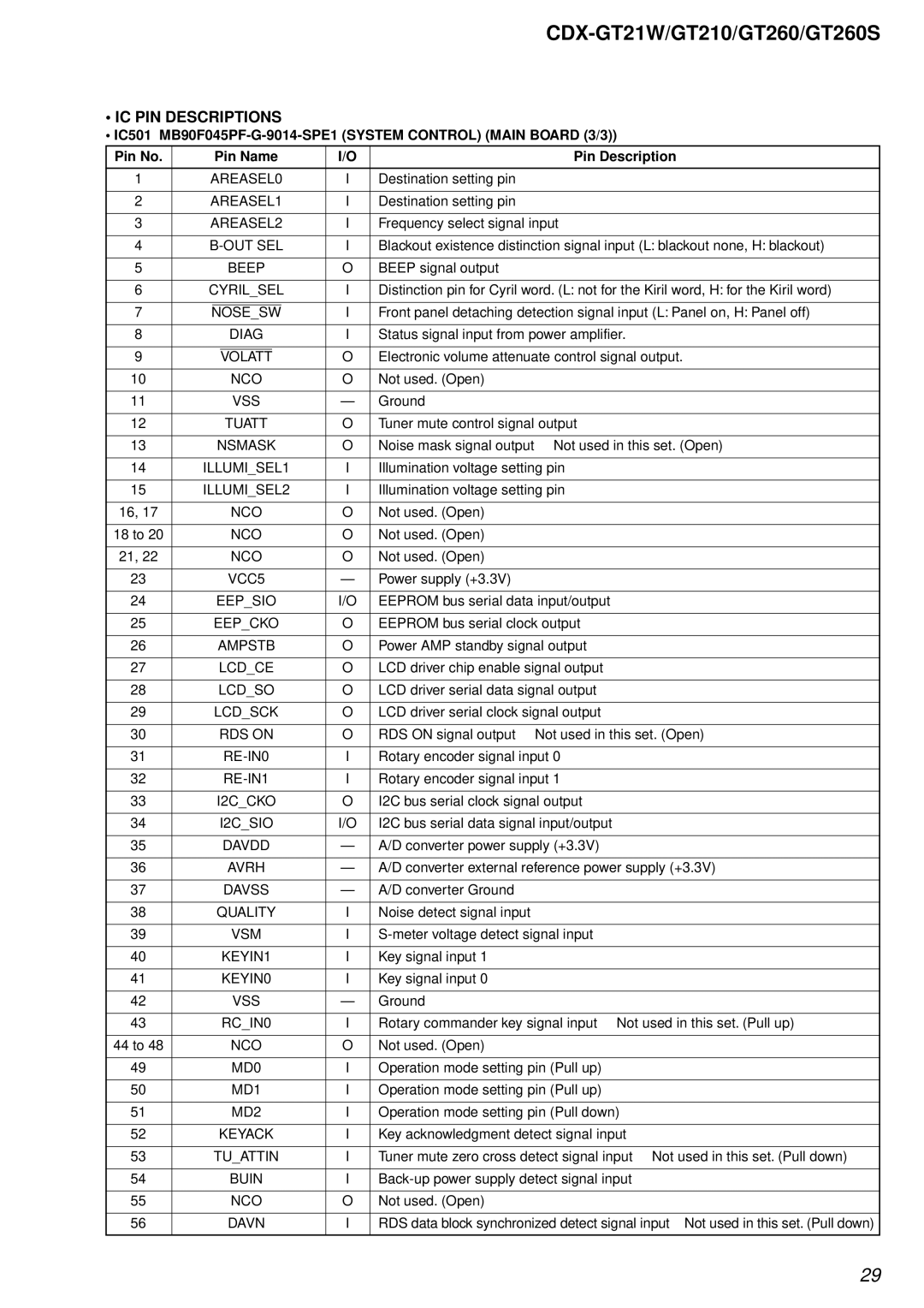
•IC PIN DESCRIPTIONS
•IC501
Pin No. |
| Pin Name | I/O |
| Pin Description | |||
|
|
|
|
|
|
|
|
|
1 | AREASEL0 | I | Destination setting pin |
| ||||
|
|
|
|
|
|
|
|
|
2 | AREASEL1 | I | Destination setting pin |
| ||||
|
|
|
|
|
|
|
| |
3 | AREASEL2 | I | Frequency select signal input | |||||
|
|
|
|
|
|
|
| |
4 | I | Blackout existence distinction signal input (L: blackout none, H: blackout) | ||||||
|
|
|
|
|
|
|
|
|
5 |
|
| BEEP | O | BEEP signal output |
| ||
|
|
|
|
|
|
|
| |
6 | CYRIL_SEL | I | Distinction pin for Cyril word. (L: not for the Kiril word, H: for the Kiril word) | |||||
|
|
|
|
|
|
|
| |
7 |
|
|
|
|
| I | Front panel detaching detection signal input (L: Panel on, H: Panel off) | |
NOSE_SW | ||||||||
|
|
|
|
|
|
|
| |
8 |
|
| DIAG | I | Status signal input from power amplifier. | |||
|
|
|
|
|
|
|
| |
9 |
|
|
|
| O | Electronic volume attenuate control signal output. | ||
|
| VOLATT | ||||||
|
|
|
|
|
|
|
|
|
10 |
|
| NCO | O | Not used. (Open) |
| ||
|
|
|
|
|
|
|
|
|
11 |
|
| VSS | — | Ground |
| ||
|
|
|
|
|
|
|
| |
12 |
|
| TUATT | O | Tuner mute control signal output | |||
|
|
|
|
|
|
|
|
|
13 |
| NSMASK | O | Noise mask signal output | Not used in this set. (Open) | |||
|
|
|
|
|
|
|
| |
14 | ILLUMI_SEL1 | I | Illumination voltage setting pin | |||||
|
|
|
|
|
|
|
| |
15 | ILLUMI_SEL2 | I | Illumination voltage setting pin | |||||
|
|
|
|
|
|
|
|
|
16, 17 |
|
| NCO | O | Not used. (Open) |
| ||
|
|
|
|
|
|
|
|
|
18 to 20 |
|
| NCO | O | Not used. (Open) |
| ||
|
|
|
|
|
|
|
|
|
21, 22 |
|
| NCO | O | Not used. (Open) |
| ||
|
|
|
|
|
|
|
|
|
23 |
|
| VCC5 | — | Power supply (+3.3V) |
| ||
|
|
|
|
|
|
|
| |
24 |
| EEP_SIO | I/O | EEPROM bus serial data input/output | ||||
|
|
|
|
|
|
|
| |
25 |
| EEP_CKO | O | EEPROM bus serial clock output | ||||
|
|
|
|
|
|
|
| |
26 |
| AMPSTB | O | Power AMP standby signal output | ||||
|
|
|
|
|
|
|
| |
27 |
| LCD_CE | O | LCD driver chip enable signal output | ||||
|
|
|
|
|
|
|
| |
28 |
| LCD_SO | O | LCD driver serial data signal output | ||||
|
|
|
|
|
|
|
| |
29 |
| LCD_SCK | O | LCD driver serial clock signal output | ||||
|
|
|
|
|
|
|
|
|
30 |
| RDS ON | O | RDS ON signal output | Not used in this set. (Open) | |||
|
|
|
|
|
|
|
| |
31 |
|
| I | Rotary encoder signal input 0 | ||||
|
|
|
|
|
|
|
| |
32 |
|
| I | Rotary encoder signal input 1 | ||||
|
|
|
|
|
|
|
| |
33 |
| I2C_CKO | O | I2C bus serial clock signal output | ||||
|
|
|
|
|
|
|
| |
34 |
| I2C_SIO | I/O | I2C bus serial data signal input/output | ||||
|
|
|
|
|
|
|
| |
35 |
|
| DAVDD | — | A/D converter power supply (+3.3V) | |||
|
|
|
|
|
|
|
| |
36 |
|
| AVRH | — | A/D converter external reference power supply (+3.3V) | |||
|
|
|
|
|
|
|
|
|
37 |
|
| DAVSS | — | A/D converter Ground |
| ||
|
|
|
|
|
|
|
|
|
38 |
| QUALITY | I | Noise detect signal input |
| |||
|
|
|
|
|
|
|
| |
39 |
|
| VSM | I | ||||
|
|
|
|
|
|
|
|
|
40 |
|
| KEYIN1 | I | Key signal input 1 |
| ||
|
|
|
|
|
|
|
|
|
41 |
|
| KEYIN0 | I | Key signal input 0 |
| ||
|
|
|
|
|
|
|
|
|
42 |
|
| VSS | — | Ground |
| ||
|
|
|
|
|
|
|
| |
43 |
|
| RC_IN0 | I | Rotary commander key signal input Not used in this set. (Pull up) | |||
|
|
|
|
|
|
|
|
|
44 to 48 |
|
| NCO | O | Not used. (Open) |
| ||
|
|
|
|
|
|
|
| |
49 |
|
| MD0 | I | Operation mode setting pin (Pull up) | |||
|
|
|
|
|
|
|
| |
50 |
|
| MD1 | I | Operation mode setting pin (Pull up) | |||
|
|
|
|
|
|
|
| |
51 |
|
| MD2 | I | Operation mode setting pin (Pull down) | |||
|
|
|
|
|
|
|
| |
52 |
| KEYACK | I | Key acknowledgment detect signal input | ||||
|
|
|
|
|
|
|
| |
53 |
| TU_ATTIN | I | Tuner mute zero cross detect signal input Not used in this set. (Pull down) | ||||
|
|
|
|
|
|
|
| |
54 |
|
| BUIN | I | ||||
|
|
|
|
|
|
|
|
|
55 |
|
| NCO | O | Not used. (Open) |
| ||
|
|
|
|
|
|
|
| |
56 |
|
| DAVN | I | RDS data block synchronized detect signal input Not used in this set. (Pull down) | |||
|
|
|
|
|
|
|
|
|
29