Sony HCD-RG40 specifications 4040, HCD-DX30/RG40, Pin No, Pin Name, Description

Models: HCD-RG40 HCD-DX30

1 64
Download 64 pages 44.84 Kb
Page 40
Image 40

HCD-DX30/RG40

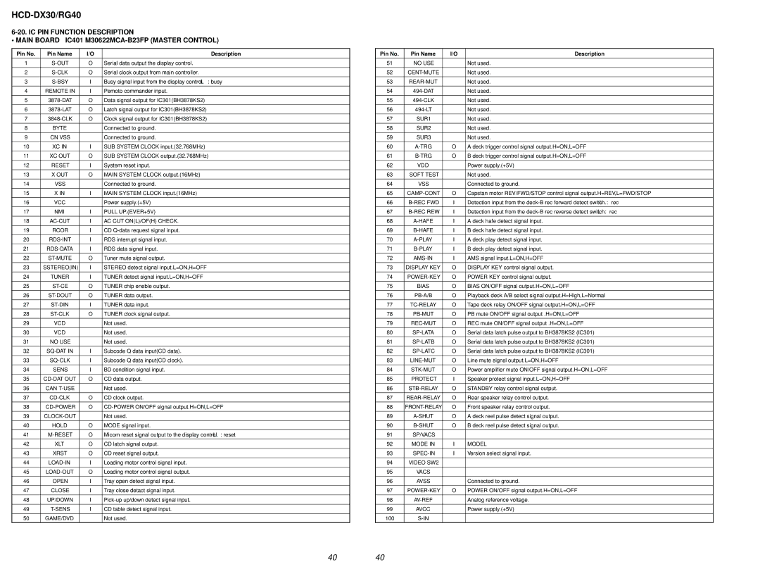
6-20. IC PIN FUNCTION DESCRIPTION

• MAIN BOARD IC401 M30622MCA-B23FP (MASTER CONTROL)

Pin No.

Pin Name

I/O

Description


1

S-OUT

O

Serial data output the display control.


2

S-CLK

O

Serial clock output from main controller.


3

S-BSY

I

Busy signal input from the display control. “L” : busy


4

REMOTE IN

I

Pemoto commander input.


5

3878-DAT

O

Data signal output for IC301(BH3878KS2)


6

3878-LAT

O

Latch signal output for IC301(BH3878KS2)


7

3848-CLK

O

Clock signal output for IC301(BH3878KS2)


8

BYTE

Connected to ground.


9

CN VSS

Connected to ground.


10

XC IN

I

SUB SYSTEM CLOCK input.(32.768MHz)


11

XC OUT

O

SUB SYSTEM CLOCK output.(32.768MHz)


12

RESET

I

System reset input.


13

X OUT

O

MAIN SYSTEM CLOCK output.(16MHz)


14

VSS

Connected to ground.


15

X IN

I

MAIN SYSTEM CLOCK input.(16MHz)


16

VCC

Power supply.(+5V)


17

NMI

I

PULL UP.(EVER+5V)


18

AC-CUT

I

AC CUT ON(L)/OF(H) CHECK.


19

RCOR

I

CD Q-data request signal input.


20

RDS-INT

I

RDS interrupt signal input.


21

RDS-DATA

I

RDS data signal input.


22

ST-MUTE

O

Tuner mute signal output.


23

SSTEREO(IN)

I

STEREO detect signal input.L=ON,H=OFF


24

TUNER

I

TUNER detect signal input.L=ON,H=OFF


25

ST-CE

O

TUNER chip eneble output.


26

ST-DOUT

O

TUNER data output.


27

ST-DIN

I

TUNER data input.


28

ST-CLK

O

TUNER clock signal output.


29

VCD

Not used.


30

VCD

Not used.


31

NO USE

Not used.


32

SQ-DAT IN

I

Subcode Q data input(CD data).


33

SQ-CLK

I

Subcode Q data input(CD clock).


34

SENS

I

BD condition signal input.


35

CD-DAT OUT

O

CD data output.


36

CAN’T-USE

Not used.


37

CD-CLK

O

CD clock output.


38

CD-POWER

O

CD-POWER ON/OFF signal output.H=ON,L=OFF


39

CLOCK-OUT

Not used.


40

HOLD

O

MODE signal input.


41

M-RESET

O

Micom reset signal output to the display control. “L” : reset


42

XLT

O

CD latch signal output.


43

XRST

O

CD reset signal output.


44

LOAD-IN

I

Loading motor control signal input.


45

LOAD-OUT

O

Loading motor control signal output.


46

OPEN

I

Tray open detect signal input.


47

CLOSE

I

Tray close detact signal input.


48

UP/DOWN

I

Pick-up up/down detect signal input.


49

T-SENS

I

CD table detect signal input.


50

GAME/DVD

Not used.


Pin No.

Pin Name

I/O

Description


51

NO USE

Not used.


52

CENT-MUTE

Not used.


53

REAR-MUT

Not used.


54

494-DAT

Not used.


55

494-CLK

Not used.


56

494-LT

Not used.


57

SUR1

Not used.


58

SUR2

Not used.


59

SUR3

Not used.


60

A-TRG

O

A deck trigger control signal output.H=ON,L=OFF


61

B-TRG

O

B deck trigger control signal output.H=ON,L=OFF


62

VDD

Power supply.(+5V)


63

SOFT TEST

Not used.


64

VSS

Connected to ground.


65

CAMP-CONT

O

Capstan motor REV/FWD/STOP control signal output.H=REV,L=FWD/STOP


66

B-REC FWD

I

Detection input from the deck-B rec forward detect switch. “L” : rec


67

B-REC REW

I

Detection input from the deck-B rec reverse detect switch. “L” : rec


68

A-HAFE

I

A deck hafe detect signal input.


69

B-HAFE

I

B deck hafe detect signal input.


70

A-PLAY

I

A deck play detect signal input.


71

B-PLAY

I

B deck play detect signal input.


72

AMS-IN

I

AMS signal input.L=ON,H=OFF


73

DISPLAY KEY

O

DISPLAY KEY control signal output.


74

POWER-KEY

O

POWER KEY control signal output.


75

BIAS

O

BIAS ON/OFF signal output.H=ON,L=OFF


76

PB-A/B

O

Playback deck A/B select signal output.H=High,L=Normal


77

TC-RELAY

O

Tape deck relay ON/OFF signal output.H=ON,L=OFF


78

PB-MUT

O

PB mute ON/OFF signal output .H=ON,L=OFF


79

REC-MUT

O

REC mute ON/OFF signal output .H=ON,L=OFF


80

SP-LATA

O

Serial data latch pulse output to BH3878KS2 (IC301)


81

SP-LATB

O

Serial data latch pulse output to BH3878KS2 (IC301)


82

SP-LATC

O

Serial data latch pulse output to BH3878KS2 (IC301)


83

LINE-MUT

O

Line mute signsl output.L=ON,H=OFF


84

STK-MUT

O

Power amplifier mute ON/OFF signal output.H=ON,L=OFF


85

PROTECT

I

Speaker protect signal input.L=ON,H=OFF


86

STB-RELAY

O

STANDBY relay control signal output.


87

REAR-RELAY

O

Rear speaker relay control output.


88

FRONT-RELAY

O

Front speaker relay control output.


89

A-SHUT

O

A deck reel pulse detect signal output.


90

B-SHUT

O

B deck reel pulse detect signal output.


91

SP/VACS


92

MODE IN

I

MODEL


93

SPEC-IN

I

Version select signal input.


94

VIDEO SW2


95

VACS


96

AVSS

Connected to ground.


97

POWER-KEY

O

POWER ON/OFF signal output.H=ON,L=OFF


98

AV-REF

Analog reference voltage.


99

AVCC

Power supply.(+5V)


100

S-IN


4040

Page 40
Image 40
Sony HCD-RG40 specifications 4040, HCD-DX30/RG40, Pin No, Pin Name, Description