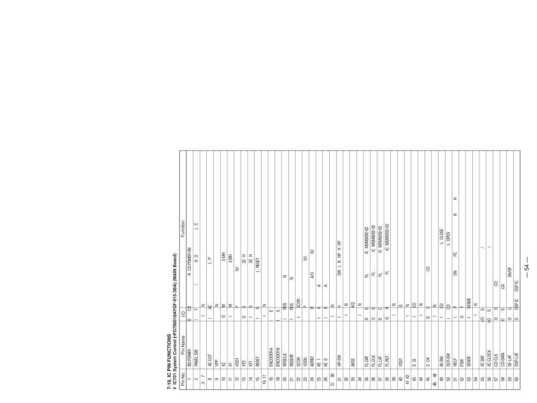
7-19. IC PIN FUNCTIONS
• IC701 System Control (∝PD780018AYGF-015-3BA) (MAIN Board)
Pin No. | Pin Name | I/O | Function |
1 | BD POWER | O | CD power control pin, “H”:CD POWER ON |
|
|
|
|
2 | PANEL SW | I | Front cover open/close switch, “H”:Open glass door, “L”:Close glass door |
|
|
|
|
3 to 7 | – | I | Not used |
|
|
|
|
8 | AC.CUT | I | AC power connection signal, “L”:Power is disconnected |
|
|
|
|
9 | VPP | – | Normally connected to the ground pin |
|
|
|
|
10 | X2 | O | Main system clock output pin (5 MHz) |
|
|
|
|
11 | X1 | I | Main system clock input pin (5 MHz) |
|
|
|
|
12 | VDD1 | – | Positive power supply (+5V) |
|
|
|
|
13 | XT2 | O | Sub system clock output pin (32 kHz) |
|
|
|
|
14 | XT1 | I | Sub system clock output pin (32 kHz) |
|
|
|
|
15 | RESET | I | System reset input pin, “L”:RESET |
|
|
|
|
16, 17 | – | I | Not used |
|
|
|
|
18 | ENCODER A | I | Encoder input pin for jogging |
|
|
|
|
19 | ENCODER B | I | Encoder input pin for jogging |
|
|
|
|
20 | RDSCLK | I | RDS clock input pin (Not used) |
|
|
|
|
21 | RDSDAT | I | RDS data input pin (Not used) |
|
|
|
|
22 | SCOR | I | SCOR input pin |
|
|
|
|
23 | VDD0 | – | Positive power supply of port (+5V) |
|
|
|
|
24 | ADREF | – | Reference voltage of A/D converter (+5V) |
|
|
|
|
25 | KEY1 | I | Key input pin (Analog input) |
|
|
|
|
26 | KEY0 | I | Key input pin (Analog input) |
|
|
|
|
27 to 30 | – | I | Not used |
|
|
|
|
31 | I | Headphone detection SW, “L”:No HP, “H”:HP | |
|
|
|
|
32 | – | I | Not used |
|
|
|
|
33 | AVSS | – | A/D converter ground potential |
|
|
|
|
34 | – | I | Not used |
|
|
|
|
35 | FL.DAT | O | Serial data output for FL tube control IC |
|
|
|
|
36 | FL.CLK | O | Serial clock output for FL tube control IC |
|
|
|
|
37 | FL.LAT | O | Chip select output for FL tube control IC |
|
|
|
|
38 | FL.RST | O | Reset signal output for FL tube control IC |
|
|
|
|
39 | – | I | Not used |
|
|
|
|
40 | VSS1 | – | Ground potential other than port and analog |
|
|
|
|
41, 42 | – | I | Not used |
|
|
|
|
43 | SQSI | I | CD sub code data input |
|
|
|
|
44 | – | I | Not used |
|
|
|
|
45 | SQCK | O | Clock output for reading CD sub code |
|
|
|
|
46 to 48 | – | I | Not used |
|
|
|
|
49 | I | CD tray close completion detection input, “L”:CLOSE | |
|
|
|
|
50 | I | CD tray open completion detection input, “L”:OPEN | |
|
|
|
|
51 | HELP | I | Pin requesting power ON from the PC link adapter (optional), Normally “H” |
|
|
|
|
52 | FSW | O | Focus gain switch |
|
|
|
|
53 | SENSE | I | SENSE input pin |
|
|
|
|
54 | – | I | Not used |
|
|
|
|
55 | IIC DAT | I/O | System control communication data input/output pin |
|
|
|
|
56 | IIC CLOCK | I/O | System control communication clock input/output pin |
|
|
|
|
57 | O | Serial clock for CD control | |
|
|
|
|
58 | O | Serial data for CD control | |
|
|
|
|
59 | O | Chip select signal for DA/DF | |
|
|
|
|
60 | O | DSP IC and SSP IC chip select | |
|
|
|
|
– 54 –