THIS NOTE IS COMMON FOR PRINTED WIRING BOARDS AND SCHEMATIC DIAGRAMS.
(In addition to this, the necessary note is printed in each block.)
For schematic diagrams.
Note:
•All capacitors are in ∝F unless otherwise noted. pF: ∝∝F 50 WV or less are not indicated except for electrolytics and tantalums.
•All resistors are in Ω and 1/4 W or less unless otherwise specified.
•f : internal component.
•C: panel designation.
Note:
The components identi- fied by mark 0or dotted line with mark 0are criti- cal for safety.
Replace only with part number specified.
•A: B+ Line.
•B: B– Line.
•H: adjustment for repair.
•Voltages and waveforms are dc with respect to ground under
no mark : STOP
( ) : PLAY
<> : REC
∗: Impossible to measure
•Voltages are taken with a VOM (Input impedance 10 MΩ). Voltage variations may be noted due to normal produc- tion tolerances.
•Waveforms are taken with a oscilloscope.
Voltage variations may be noted due to normal produc- tion tolerances.
•Circled numbers refer to waveforms.
•Signal path.
E : PB
j : REC
p : PB (DIGITAL OUT)
l: REC (DIGITAL IN)
•Abbreviation
SP : Singapore model
For printed wiring boards.
Note:
•X: parts extracted from the component side.
•Y: parts extracted from the conductor side.
•a : Through hole.
•b: Pattern from the side which enables seeing. (The other layers' patterns are not indicated.)
Caution:
Pattern face side: Parts on the pattern face side seen from the
(Side B) pattern face are indicated.
Parts face side: Parts on the parts face side seen from the
(Side A) | parts face are indicated. |
B C E
These are omitted.
B C E
These are omitted.
C ![]()
|
|
|
|
|
|
|
|
|
|
|
|
|
| Q |
|
| These are omitted. | ||||
|
|
|
|
| ||||||
B E
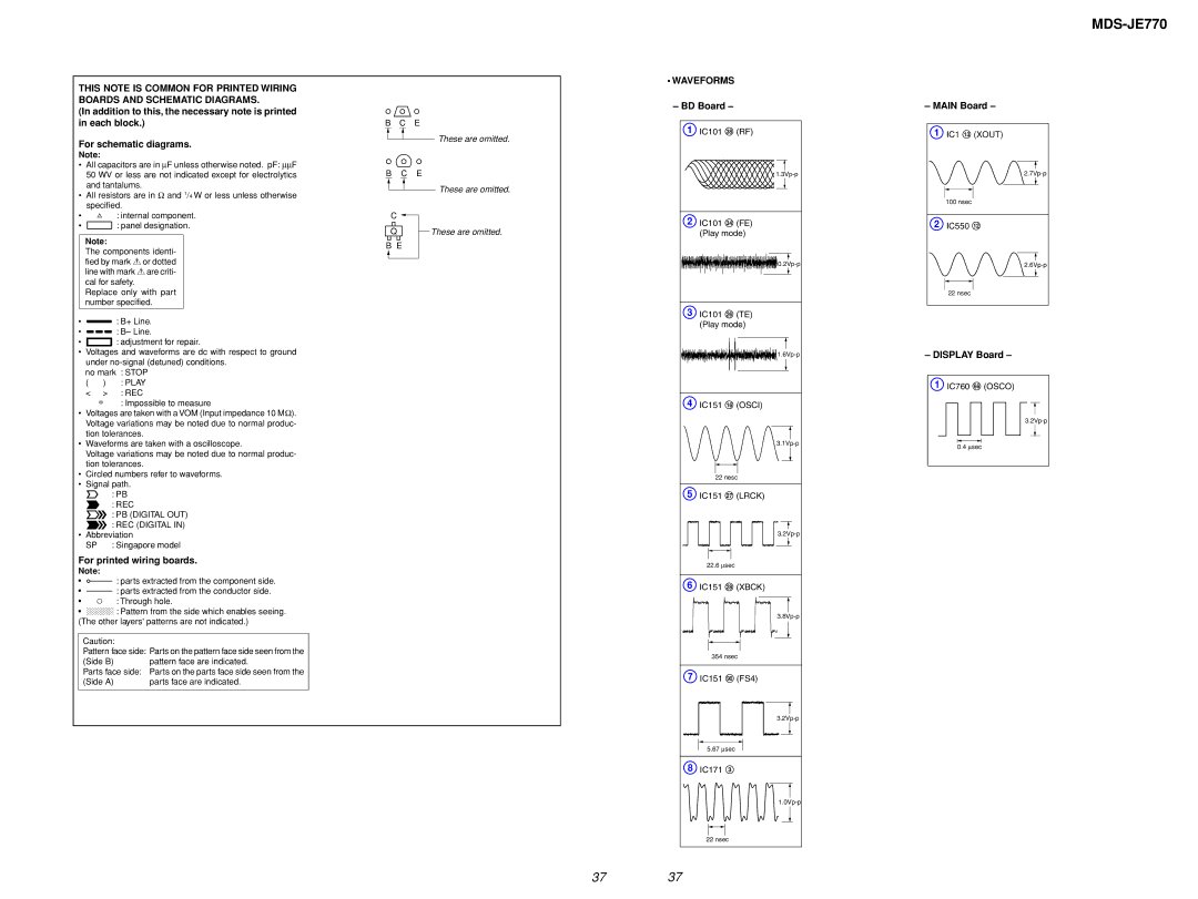
•WAVEFORMS
–BD Board –
1 IC101 ek (RF)
2 IC101 ef (FE) (Play mode)
3 IC101 wh (TE) (Play mode)
4 IC151 qh (OSCI)
22 nesc
5 IC151 wj (LRCK)
22.6 ∝sec
6 IC151 wk (XBCK)
354 nsec
7 IC151 o; (FS4)
5.67 ∝sec
8 IC171 3
22 nsec
37 37
MDS-JE770
– MAIN Board –
1 IC1 qd (XOUT)
100 nsec
2 IC550 qs
22nsec
–DISPLAY Board –
1 IC760 yh (OSCO) |
0.4 ∝sec |